


Theory of Operation
AM700 Audio Measurement Set Service Manual
3–71
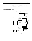
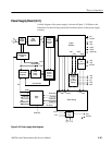
+5 V output voltage and information about the current in L4 to control pulse-
width modulation of the preregulator. On pins 8 and 9 of U1, C20 and R12 set
the frequency of operation at approximately 100 kHz. Pin 2 of U1 is a +5 V,
±5 mV voltage reference.
The +5 V output of the supply is divided to 2.5 V by R21 and R22 and applied
to the error amplifier that is internal to U1 at pin 6 (– pin). Pin 5, the + pin of the
error amplifier, is the reference voltage for the error amplifier. The regulating
point for the +5 V output is set by R14, a variable potentiometer that adjusts the
reference voltage on pin 5. Compensation and feedback for the error amplifier is
provided by C23.
Comp Out, pin 7, is also used for regulation sensing. That level is compared by
U48 with a divided down Vref. The Comp Out level on the inverting input of
U48 is normally higher than the input on the non-inverting input, so RDETECT
will be low during normal operation. When the PWM reaches its drive limit, the
output state of U48 switches to high. That high biases on CR32 to pass the
RDETECT signal to the Power Supply Supervisor, U9. That device then issues a
POWER FAIL signal to the CPU so that writing to the NVRAM is halted before
the power supply goes out of regulation.
The current information of L4 from the Current Sensing circuit is applied as a
trapezoidal-type waveform to U1 at pin 4. Transistor Q1 adds a small portion of
the timing ramp on pin 8 to the current signal at pin 4 to improve noise
immunity and to set the PWM correctly for current-mode operation. Both these
signals, the +5 V feedback at pin 6 and the current signal with the added ramp at
pin 4, must be present for U1 to work properly.
A shutdown signal, OVSD OR’ed with SD and applied to pin 16 of U1, is used
to turn off the Pulse-Width Modulator. The SD signal is developed by the
Shutdown Gate, U18B, in the Alarm Logic circuitry. The SD signal is high when
the power STBY/ON switch is in STBY and for a number of irregular conditions
of the power supply (overvoltage, over temperature, or overcurrent).
The OVSD (overvoltage shutdown) signal is developed by VR2, Q11, and
U15B. The OVSD signal is low through inverter U16B unless the +5 V becomes
high enough to fire Q11 (about 6 V) and remove the low from the OVSD signal
line. The two signals are diode-OR’ed to provide the shutdown signal to U1.
When neither the OVSD nor the SD signal is high, the shutdown inhibit is
removed from U1 to permit the PWM to begin operation. If either signal is high,
the associated diode (CR12 or CR13) conducts to bias on CR14. This pulls pin
16 of U1 high to inhibit it from running, shutting down the power supply.
Jumper J3 is for testing purposes only. It may be pulled to eliminate the SD
signal for testing of the PWM during troubleshooting, but this also eliminates all
the shutdown control by the control logic circuitry except for the overvoltage
shutdown. Troubleshooting should be attempted only by an experienced service
person.