


Theory of Operation
AM700 Audio Measurement Set Service Manual
3–23
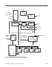
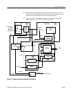
The DSP Address Decoder, U5, is a PAL device. It looks at nine selected DSP
address lines and three of the Data and Address bus control pins, (DPS), (DDS),
and X/Y, and decodes them to produce chip enable control signals: (RAM_CE),
(SID_CE), (STX_CE), (PHASE_CE), (ENCJIT_CE), and (COUNT_CE). DSP
RAM address lines RA15 and RA16 are also decoded here.
A crystal clock circuit, Y1, supplies a 12.288 MHz OSC signal to the timing
generator PAL circuit that produces the DSPCLK signal. That clock signal is
multiplied by the DSP to provide an internal DSP clock of 39.74 MHz.
There is a interrupt to the DSP that is used when jittering the digital output
signal. This interrupt comes at a constant rate to add jitter to the digital output
signal for testing the jitter immunity of a device under test.
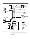
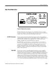
Synchronous Serial Interface (SSI) (diagram 2)
Interfacing the serial DSP port on the rear panel to the DSP SSI is done by U59,
the SSI control PAL. The audio sample bits are generated directly at the DSP,
and the control PAL outputs the digital signals with the surrounding bits that are
required for digital signal formats. The control PAL selects whether the clocks
are derived from the generator or the external port. When receiving or sending
digital data through the DSP port, the clock to the SSI shift register is supplied
by the external device.
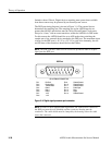
Sample Transmitter (diagram 3)
The Sample Transmitter formats data from the Main and Reference receivers into
a form that can be applied to the DSP.
A simplified block diagram of the Sample Transmitter was shown previously in
Figure 3–4. The formatted serial data is received from the Format PAL. That data
is then arranged into eight-bit data bytes to be sent to the DSP. A block of nine
bytes is sent to the DSP. The first byte defines the channel source of the data; the
remaining eight bytes are 32 bits of left data followed by 32 bits of right data. A
Start bit, TIDENT, goes high at the first byte, then low for the remaining bytes of
the data block. The data is clocked into the DSP by the TCLK signal.
Address Decoder
DSP Clock
Jitter Interrupt
Sample Transmitter