


Theory of Operation
3–22
AM700 Audio Measurement Set Service Manual
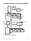
DSP RESET. At power up, the DSP is held in reset until the power and PLL has
stabilized. The RESET input is a Schmitt trigger. When (DSPRST) is asserted
(low), the DSP is initialized and placed into the reset state. The DSPRST signal
is widespread throughout the Digital Audio board.
Mode/(IRO) Lines. After the DSP leaves the reset state, the mode setting input
pins are switched to interrupt request inputs (IRQA, IRQB, and NMI). IRQA and
IRQB can be programmed to be level sensitive or negative edge triggered. NMI
(non-maskable interrupt) is negative edge triggered and triggering occurs at a
voltage level.
Analog PLL Pins. The DSP PLL has dedicated power and ground pins. These pins
are connected to the common +5 V supply and the common digital ground for
the DSP chip. The PLL output clock, CKOUT is a 50% duty cycle clock that is
synchronized to the internal processor clock when the PLL is enabled and
locked. The CKOUT polarity control pin (CKP) is strapped to ground through
R7 to make the CKOUT polarity the same as the EXTAL DSPCLK signal. The
PLL initialization input, PINIT, is pulled up to +5 V through R6 to permanently
enable the PLL. During hardware reset, the high value of the PINIT pin causes
the internal clocks to be derived from the PLL VCO output. After hardware
reset, the state of the PINIT pin is ignored. When the PLL is locked to the proper
phase and frequency of the EXTAL input clock, the PLOCK signal is asserted
and the PLL Locked LED, DS1, will be on. This is a reliable indication of lock
only after the hardware reset is exited.
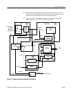
The CPU and the DSP communicate through the host interface. Two buffers
between the CPU and the DSP isolate the two devices from each other when they
are not communicating. Data is passed both ways by U99, a bidirectional octal
buffer. Control signals and addresses from the CPU are buffered by U100. The
control signals and the addresses are separately enabled in U100. The control
signals are permanently enabled, but the address bits are not enabled through
U100 until the CPU places addresses on the address inputs pins and issues the
(SBIT) signal. That same signal also enables the data buffer, U99, to pass data in
the direction selected by the HR/(W) control bit from U100.
The DSP RAM, a SIMM device, U98, provides the memory storage space
needed for holding the processed digital data. Read and write control signals
from the DSP control the direction of data flow. The RAM is enabled by the
(RAM CE) signal from address decoder U5. The RAM chip is a 32 bit device,
but only 24 data bits are used. The remaining bits are pulled up to +5 V through
a pull-up resistor pack, R223.
Host Interface Buffers
DSP RAM