


Theory of Operation
3–12
AM700 Audio Measurement Set Service Manual
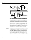
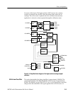
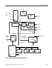
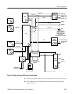
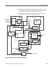
Calibration, Control Registers, Interface, and Power Supplies (diagram 6)
Refer to schematic diagram 6 of the A1A1 circuit board for the following circuit
description. The circuitry shown on this diagrams is composed of unrelated
circuitry that includes the calibration test signal generator, the TTL trigger input
circuit, the isolated power supplies for the A/D Converters, and a 72-bit serial
control register used to store the controlling signals for switching the attenuators,
gain settings, and input terminations. Other control bits determine the setting of
the notch filter frequency and control the calibration sine-wave oscillator and
square-wave chopper.
Two calibration signals to the analog acquisition circuitry are provided. One is a
5 V, 120 Hz, symmetrical square-wave signal. The other is a highly accurate
±2.5 V sine wave. The square-wave signal is produced by chopping between a
precision 5 V voltage reference and ground. When this precise duty-cycle square
wave is AC-coupled, it provides a ±2.5 V reference used to calibrate the gain of
the A/D Convertors and signal path.
A test point, TP31, is provided to check this signal using an oscilloscope. Test
points are also provided to check the precision 5 V reference and the output of
the sine-wave oscillator. Switching relays under control of signals from the
Serial Control Register are applied to a relay driver, U82, to select the calibration
signals and direct them to the channel being calibrated. During calibration, offset
and gain calibration constants are derived. These are used to correct offset and
gain shifts due to thermal effects and component aging. Maximum accuracy for
measurements is obtained immediately after a calibration cycle.
The Control Register, U116, is a 72 bit serial register. It is formed by a series of
registers mounted on a SIMM chip. Serial control data bits are loaded from the
DSP. When any control bit is changed, all 72 bits must be re-sent to the register,
but when the data is latched, only those bits that have changed are written to the
register output pins.
Power to the isolated power supply is provided from the + and –15 V sources.
Test points are provided to check these inputs. These inputs are also separately
fused on the board by 5 A fuses, F3 and F4. Additional filtering is done on each
side of these sources before being applied to three-terminal regulators. There are
two three-terminal regulators with + 5 V output and two more with –5 V output.
Test points are provided on each of these outputs to verify the voltage levels. The
isolated supplies are used to provide power to the A/D Converters to limit the
introduction of noise to the converters.
Interface status reports under- and over-range conditions, CAL BUSY, and input
overload conditions. The status bits are parallel loaded in read-back register
U109 and clocked out serially. There is also a read-back signal that is serially
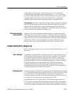
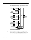
Calibration Signal Source
Serial Control Register
Isolated Power Supply
Interface Status
Read-back Register