


Theory of Operation
3–10
AM700 Audio Measurement Set Service Manual
96 kHz, the roll off is better than 90 dB. A servo circuit following the filter
(U122 and associated components), looks at the DC offset of the output and
feeds back an offsetting signal to the filter. At the output of the filter, the DC
offset is reduced to a few millivolts.
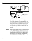
In the High Bandwidth A/D Converters, the left and right signals are applied
single-ended. Both channels also have separate serial data outputs instead of
being interleaved as in the High Resolution A/D Converter.
This device provides the clocking signals to the High Bandwidth A/D Converter.
Although the decimated data from the A/D is derived, it is not currently used by
the AM700 software.
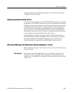
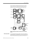
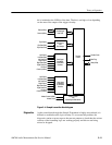
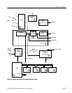
Sample Transmitter (diagram 5)
A simplified block diagram of the Sample Transmitter is shown in Figure 3–4.
The Sample Transmitter formats data from the A/D Converters into a form that
can be applied to the DSP. Data from the A/D Converters does not follow a
standard format, and both A/D Converters, High Resolution and High Band-
width, output data in different formats. This means that each data stream must be
reformatted into a pattern that the Sample Transmitter ASIC, U120, can use.
Both transmit and receive capabilities are included in the Sample Transmitter
ASIC. A single bit is set to switch between using the device as a transmitter or as
a receiver. Refer to schematic diagram 5 of the A1A1 circuit board for the
following circuit description.
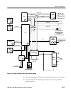
These PALs, U117, U118, and U119, accept data from the A/D Converters and
format it into data streams that contain a Start bit, a Stop bit, and the appropriate
number of bits between that are the digitized audio signal. A second job of these
PALs is to accept the eight bits that define the gain and attenuation settings and
encode them into a four-bit signal that tells the Sample Transmitter ASIC how
much shift is needed to restore the actual input audio signal level.
The formatted serial data is received from the Format PALS and shifted as
necessary to remove the gain and attenuation from the signal that was applied
prior to being digitized by the A/D Converters. That data is then arranged into
eight-bit data bytes to be sent to the DSP. A block of nine bytes is sent to the
DSP. The first byte defines the channel source of the data; the remaining eight
bytes are 32 bits of left data followed by 32 bits of right data. A Start bit,
TIDENT, goes high at the first byte, then low for the remaining bytes of the data
block. The data is clocked into the DSP by the TCLK signal. (In the block
diagram of Figure 3–4, this is block labeled Transfer Control.) Those signals are
applied to the DSP board through connector J26, shown on diagram 6. A trigger
High Bandwidth A/D
Converter
Decimating Filter
Format PALS
Sample Transmitter