Theory of Operation
AM700 Audio Measurement Set Service Manual
3–35
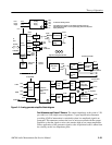
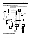
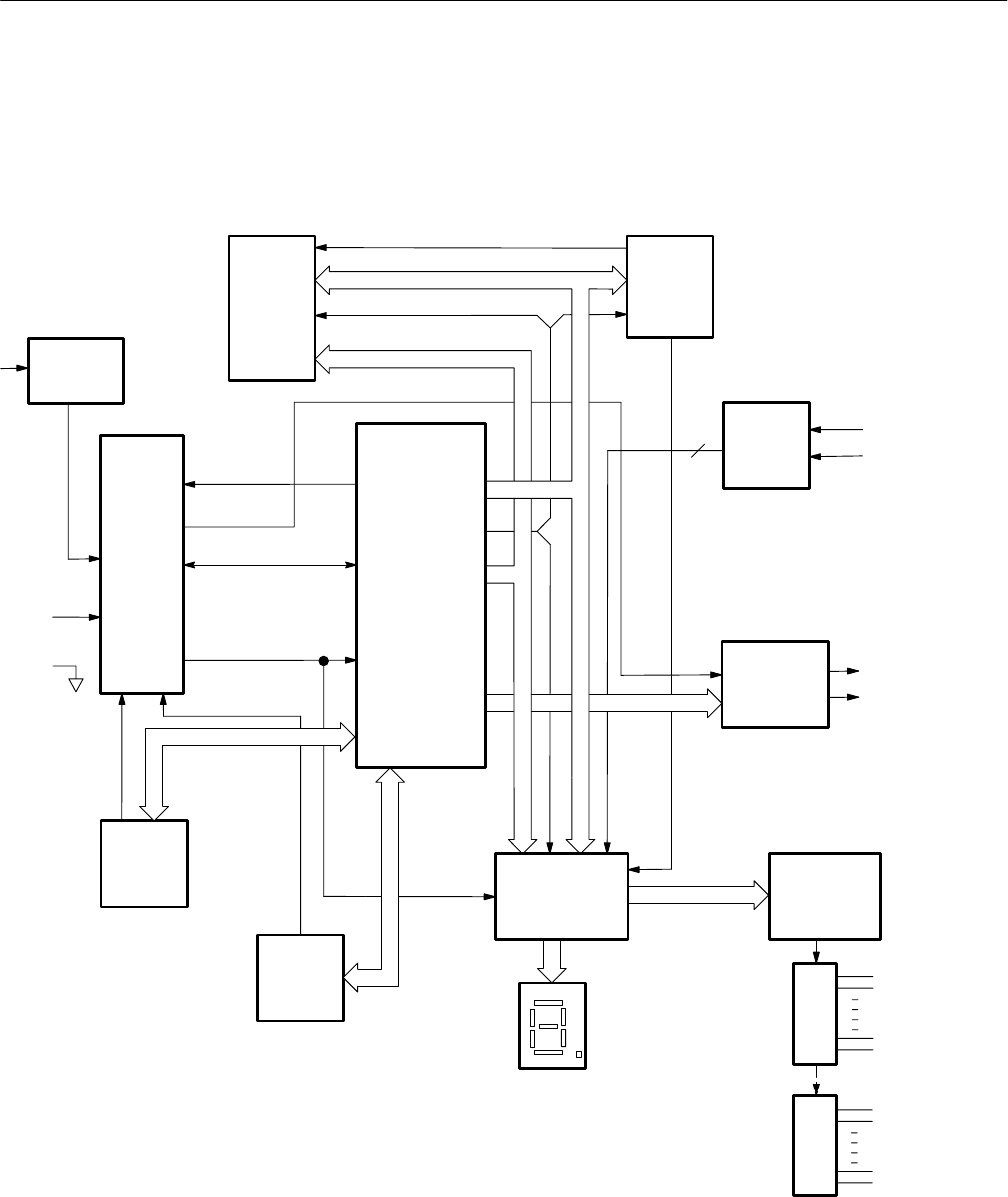
Digital Signal Processor (Generator) (diagram 1)
Refer to schematic diagram 2 of the A5 analog generator circuit board for the
following circuit description.
Once
DSP
RAM
12.288 MHz
U6
Reset
and
SSI
Clock
U7
Reset
PAL
Select
J15
RST
J4
Host
J17
Port
SCK
Disable
BCLK
SCK
DSPreset
Reset_Gen
U4
U2
SSI
CEPO
U5
Address
Decoder
PAL
U94
Opto–
Isolators
Output
Overload
To DACs
U20,U21
Clock
and
Data Isolators
Clock
and
Data Isolators
U9,U10
Serial Control
Output and ID
PAL
U87
Control
Latches
Control
Latches
Decimal Point is
Power ON Indicator
CONTROLS:
Gain
Bandpass Filter
High Res/High BW Mode
Source Impedance
To Controls
Serial
Control
Register
Data
Address
Address
BCLK
CERAM
CEPO
OVLD
Control
A(0 –15)
D(0 – 23)
2
Figure 3–12: Analog generator DSP section block diagram


