


3-32 Intel® PXA255 Processor Developer’s Manual
Clocks and Power Manager
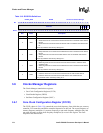
This is a read/write register. Ignore reads from reserved bits. Write zeros to reserved bits.
This is a read/write register. Ignore reads from reserved bits. Write zeros to reserved bits.
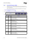
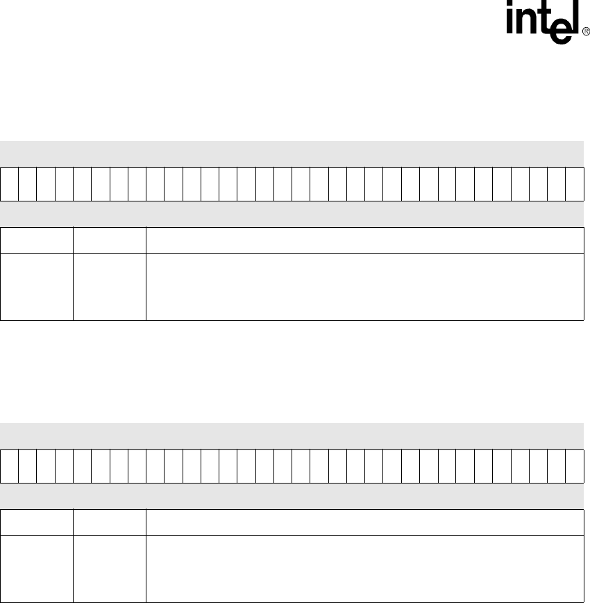
Table 3-16. PGSR0 Bit Definitions
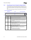
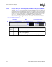
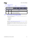
0x40F0_0020 PGSR0 Clocks and Power Manager
Bit
31 30 29 28 27 26 25 24 23 22 21 20 19 18 17 16 15 14 13 12 11 10 9 8 7 6 5 4 3 2 1 0
SS31
SS30
SS29
SS28
SS27
SS26
SS25
SS24
SS23
SS22
SS21
SS20
SS19
SS18
SS17
SS16
SS15
SS14
SS13
SS12
SS11
SS10
SS9
SS8
SS7
SS6
SS5
SS4
SS3
SS2
SS1
SS0
Reset 0 0 0 0 0 0 0 0 0 0 0 0 0 0 0 0 0 0 0 0 0 0 0 0 0 0 0 0 0 0 0 0
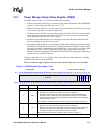
Bits Name Description
[31:0] SSx
If programmed as an output, Sleep state of GPx
0 – Pin is driven to a zero during sleep mode
1 – Pin is driven to a one during sleep mode
Cleared by hardware, watchdog, and GPIO resets.
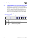
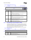
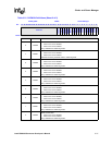
Table 3-17. PGSR1 Bit Definitions
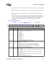
0x40F0_0024 PGSR1 Clocks and Power Manager
Bit
31 30 29 28 27 26 25 24 23 22 21 20 19 18 17 16 15 14 13 12 11 10 9 8 7 6 5 4 3 2 1 0
SS63
SS62
SS61
SS60
SS59
SS58
SS57
SS56
SS55
SS54
SS53
SS52
SS51
SS50
SS49
SS48
SS47
SS46
SS45
SS44
SS43
SS42
SS41
SS40
SS39
SS38
SS37
SS36
SS35
SS34
SS33
SS32
Reset 0 0 0 0 0 0 0 0 0 0 0 0 0 0 0 0 0 0 0 0 0 0 0 0 0 0 0 0 0 0 0 0
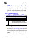
Bits Name Description
[31:0] SSx
If programmed as an output, Sleep state of GPx
0 – Pin is driven to a zero during sleep mode
1 – Pin is driven to a one during sleep mode
Cleared by hardware, watchdog, and GPIO resets.