


7-44 Intel® PXA255 Processor Developer’s Manual
LCD Controller
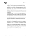
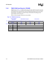
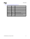
7.7 LCD Controller Register Summary
Table 7-16 shows the registers associated with the LCD Controller and the physical addresses used
to access them. All of the LCD registers must be accessed as 32-bit values.
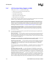
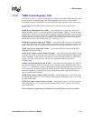
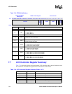
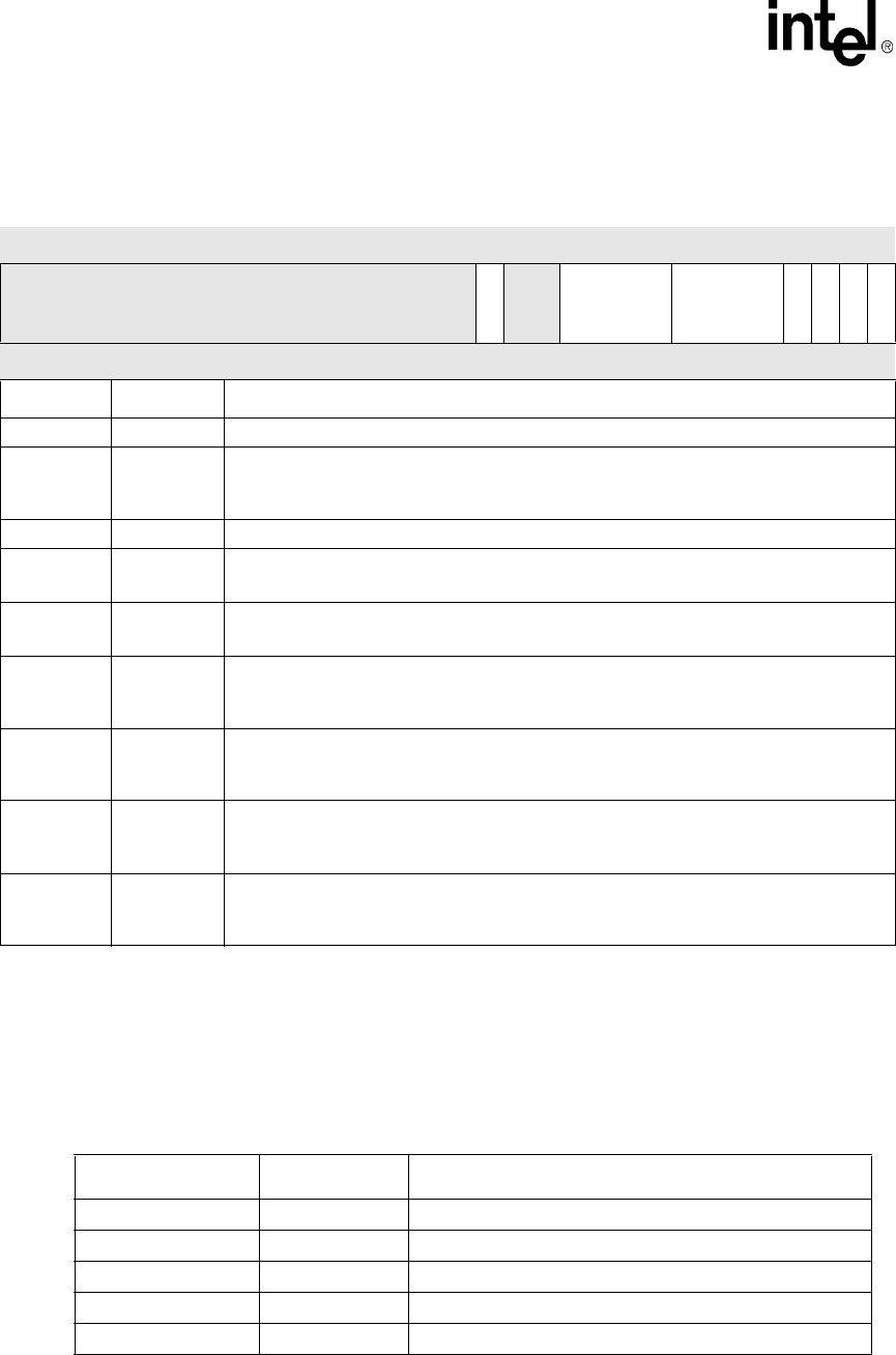
Table 7-15. TCR Bit Definitions
Physical Address
0X4400_0044
TMED Control Register LCD Controller
Bit
31 30 29 28 27 26 25 24 23 22 21 20 19 18 17 16 15 14 13 12 11 10 9 8 7 6 5 4 3 2 1 0
reserved
TED
reserved
THBS TVBS
FNAME
COAE
FNAM
COAM
Reset X X X X X X X X X X X X X X X X X 1 1 1 0 1 0 1 0 1 0 0 1 1 1 1
Bits Name Description
31:15 — reserved
14 TED
TMED Energy Distribution Matrix Select
0 = Selects Matrix 1
1 = Selects Matrix 2
13:12 — reserved
11:8 THBS
TMED Horizontal Beat Suppression
Specifies the column shift value.
7:4 TVBS
TMED Vertical Beat Suppression
Specifies the block shift value.
3FNAME
TMED Frame Number Adjuster Enable
0 = Disable frame number adjuster.
1 = Enable frame number adjuster.
2COAE
TMED Color Offset Adjuster Enable
0 = Disable color offset adjuster.
1 = Enable color offset adjuster.
1FNAM
TMED Frame Number Adjuster Matrix
0 = Selects Matrix 1 for frame number adjuster.
1 = Selects Matrix 2 for frame number adjuster.
0COAM
TMED Color Offset Adjuster Matrix
0 = Selects Matrix 1 for color offset adjuster.
1 = Selects Matrix 2 for color offset adjuster.
Table 7-16. LCD Controller Register Summary (Sheet 1 of 2)
Address Name Description
0x4400_0000 LCCR0 LCD controller control register 0
0x4400_0004 LCCR1 LCD controller control register 1
0x4400_0008 LCCR2 LCD controller control register 2
0x4400_000C LCCR3 LCD controller control register 3
0x4400_0020 FBR0 DMA channel 0 frame branch register