


Intel® PXA255 Processor Developer’s Manual 7-31
LCD Controller
where
LCLK = LCD/Memory Clock
PCD = LCCR3[7:0]
This is a read/write register. Ignore reads from reserved bits. Write zeros to reserved bits.
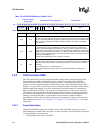
PixelClock
LCLK
2 PCD 1+()
------------- -----------------=
PCD
LCLK
2 PixelClock()
------------- ------------------------ 1–=
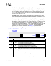
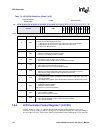
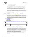
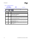
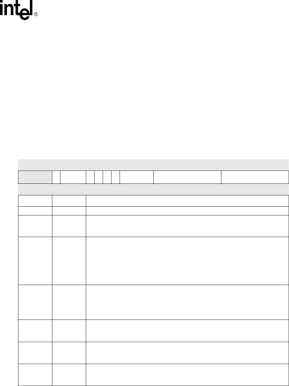
Table 7-6. LCCR3 Bit Definitions (Sheet 1 of 2)
Physical Address
0x4400_000C
LCD Controller Control Register 3 LCD Controller
Bit
31 30 29 28 27 26 25 24 23 22 21 20 19 18 17 16 15 14 13 12 11 10 9 8 7 6 5 4 3 2 1 0
reserved
DPC
BPP
OEP
PCP
HSP
VSP
API ACB PCD
Reset
X X X X 0 0 0 0 0 0 0 0 0 0 0 0 0 0 0 0 0 0 0 0 0 0 0 0 0 0 0 0
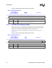
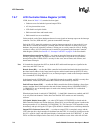
Bits Name Description
31:28 - reserved
27 DPC
Double Pixel Clock mode:
0 = The L_PCLK pin is driven at the frequency specified by PCD.
1 = The L_PCLK pin is driven at double the frequency specified by PCD.
26:24 BPP
Bits Per Pixel:
000 – 1-bits/pixel [4 entry, 8 byte palette buffer (only first 2 entries are used)]
001 – 2-bits/pixel [4 entry, 8 byte palette buffer]
010 – 4-bits/pixel [16 entry, 32 byte palette buffer]
011 – 8-bits/pixel [256 entry, 512 byte palette buffer]
100 – 16-bits/pixel [no palette buffer]
101, 110, 111 – reserved
23 OEP
Output Enable Polarity:
0 = L_BIAS pin is active high and inactive low in active display mode.
1 = L_BIAS pin is active low and inactive high in active display mode.
In active display mode, data is driven out to the LCD’s data pins on the programmed pixel
clock edge when the L_BIAS pin is active. OEP is ignored in passive display mode.
22 PCP
Pixel Clock Polarity:
0 = Data is sampled on the LCD data pins on the rising edge of L_PCLK.
1 = Data is sampled on the LCD data pins on the falling edge of L_PCLK.
21 HSP
Horizontal Sync Polarity:
0 = L_LCLK pin is active high and inactive low.
1 = L_LCLK pin is active low and inactive high.
20 VSP
Vertical Sync Polarity:
0 = L_FCLK pin is active high and inactive low.
1 = L_FCLK pin is active low and inactive high.