


6-50 Intel® PXA255 Processor Developer’s Manual
Memory Controller
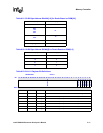
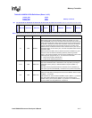
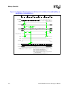
Table 6-25 provides a comparison of supported Asynchronous Static Memory types.
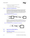
6.7.4 ROM Interface
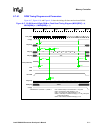
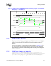
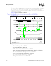
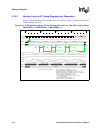
The processor provides programmable timing for both burst and non-burst ROMs. The RDF field
in MSCx is the latency (in memory clock cycles) for the first, and all subsequent, data beats from
non-burst ROMs, and the first data beat from a burst ROM. RDN is the latency for the burst data
beats after the first for burst ROMs. RRR delays the following access to a different memory space
to allow time for the current ROM to three-state the data bus.
RRR must be programmed with the maximum t
OFF
value, as specified by the ROM manufacturer.
For hardware reset initialization values, refer to Section 6.8. MSC0[15:0] is selected when the
address space corresponding to nCS0 is accessed. The processor supports a ROM burst size of 1, 4,
or 8 by configuring the MSCx[RTx] register bits to 0, 2 or 3 respectfully.
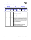
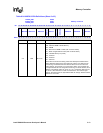
Table 6-25. Asynchronous Static Memory and Variable Latency I/O Capabilities
MSCx[RTx]
Device
Type
Timing (Memory Clocks)
Burst
Read
Address
Assert
nOE
Assert
Burst
nOE
Deassert
Burst
Write
Address
Assert
nWE
Assert
Burst
nWE
De-
assert
000
Non-burst
ROM or
Flash
RDF+1 RDF+1 0 N/A RDF+1 N/A
001 SRAM RDF+1 RDF+1 0 RDN+2 RDN+1 1
010
Burst-of-4
ROM or
Flash (non-
burst writes)
RDF+1
(0,4)
RDN+1
(1:3,5:7)
RDF+1
(0,4)
RDN+1
(1:3,5:7)
0 N/A RDF+1 N/A
011
Burst-of-8
ROM or
Flash
(non-burst
writes)
RDF+1
(0)
RDN+1
(1:7)
RDF+1
(0)
RDN+1
(1:7)
0 N/A RDF+1 N/A
100
Variable
Latency I/O
RDF+
RDN+2+waits
RDF+1+
waits
RDN+2
RDF+
RDN+2+waits
RDF+1+
waits
RDN+2