


Intel® PXA255 Processor Developer’s Manual 6-53
Memory Controller
6.7.5 SRAM Interface Overview
The processor provides a 16-bit or 32-bit asynchronous SRAM interface that uses the DQM pins
for byte selects on writes. nCS[5:0] select the SRAM bank. nOE is asserted on reads and nWE is
asserted on writes. Address bits MA[25:0] allow up to 64 Mbytes of SRAM per bank to be
addressed.
The timing for a read access is identical to that for a non-burst ROM (see Section 6.7.4.1). The
RDF fields in the MSCx registers select the latency for a read access. The MSCx[RDN] field
controls the nWE low time during a write cycle. MSCx[RRR] is the time from nCS deassertion
after a memory access to the start of another memory access. MSCx[RTx] must be configured to
0b001 to select SRAM.
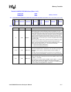
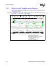
6.7.5.1 SRAM Timing Diagrams and Parameters
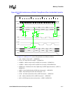
As shown in Figure 6-17, SRAM reads have the same timing as non-burst ROMs, except
DQM[3:0] are used as byte selects. For all reads, DQM[3:0] are 0b0000. During writes, all 32 data
pins are actively driven by the processor regardless of the state of the individual DQM pins.
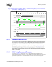
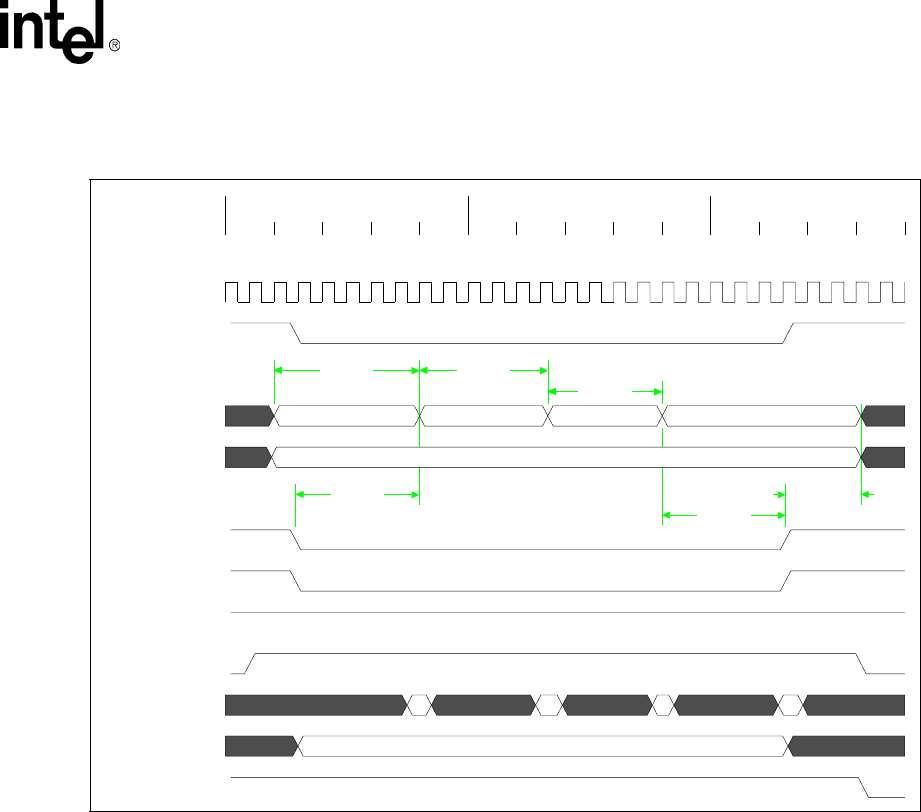
Figure 6-19. 32-Bit Non-burst ROM, SRAM, or Flash Read Timing Diagram - Four Data Beats
(MSC0[RDF] = 4, MSC0[RRR] = 1)
0 1 2 3
00
0000
RDF+1
RRR*2+1RDF+1
RDF+1RDF+1
RDF+1RDF+2 RDF+1RDF+2
MEMCLK
nCS[0]
MA[25:2]
MA[1:0]
nADV(nSDCAS)
nOE
nWE
RDnWR
MD[31:0]
DQM[3:0]
nCS[1]