6-28 Intel® PXA255 Processor Developer’s Manual
Memory Controller
The programmable opcode for address bits MA<24:17> used during the mode-register set
command (MRS) is exactly what is programmed in the MDMRS register.
6.5.7 SDRAM Waveforms
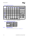
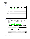
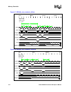
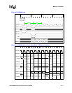
Normal operation of the SDRAM controller is shown in Figure 6-5 through Figure 6-11.
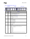
Table 6-11. SDRAM Command Encoding
Command
Pins
SDCKE
(at clk
n-1)
SDCKE
(at clk
n)
nSDCS
3:0
nSDRAS nSDCAS nWE
DQM
3:0
MA <24:10>
24:23 22:21 20 19:10
PWRDN 101 1 111 x
PWRDNX 011 1 111 x
SLFRSH 100 0 010 x
CBR 110 0 01x x
MRS 1 x 0 0 0 0 0 OP code
ACT 1 x 0 0 1 1 x bank row
READ 1 x 0 1 0 1 0 bank col 0 col
WRITE 1 x 0 1 0 0 mask bank col 0 col
PALL
PRE
All
1x0 0 10x
x
x
1
x
Bank bank 0
NOP 1x
1x xx
xx
01 11
Table 6-12. SDRAM Mode Register Opcode Table
Address Bits Option Value
MA<24:17> reserved MDMRSx
MA[16:14]
CAS Latency = 2 010
CAS Latency = 3 011
MA[13] Sequential Burst 0
MA[12:10] Burst Length = 4 010


