


12-46 Intel® PXA255 Processor Developer’s Manual
USB Device Controller
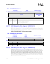
12.6.17 UDC Endpoint x Data Register (UDDR1/6/11)
UDDR1/6/11, shown in Table 12-28, is a double-buffered bulk IN endpoint that is 64 bytes deep.
Data can be loaded via DMA or direct core writes. Because it is double buffered, up to two packets
of data may be loaded for transmission.
These are write-only registers. Write zeros to reserved bits.
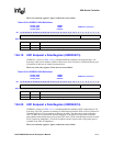
12.6.18 UDC Endpoint x Data Register (UDDR2/7/12)
UDDR2/7/12, shown in Table 12-29, is a double-buffered bulk OUT endpoint that is 64 bytes
deep. The UDC will generate either an interrupt or DMA request as soon as the EOP is received.
Since it is double buffered, up to two packets of data may be ready. Via DMA or by direct read
from the core, the data can be removed from the UDC. If one packet is being removed and the
packet behind it has already been received, the UDC will issue a NAK to the host the next time it
sends an OUT packet to endpoint(x). This NAK condition will remain in place until a full packet
space is available in the UDC at Endpoint(x).
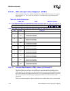
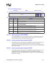
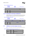
Table 12-27. UDDR0 Bit Definitions
0x 4060_0080 UDDR0 USB Device Controller
Bit
31 30 29 28 27 26 25 24 23 22 21 20 19 18 17 16 15 14 13 12 11 10 9 8 7 6 5 4 3 2 1 0
reserved
Bottom of Endpoint 0 FIFO
(for Reads) Top of
Endpoint 0 FIFO (for
Writes)
Reset
x x x x x x x x x x x x x x x x x x x x x x x x 0 0 0 0 0 0 0 0
Bits Name Description
31:8 — reserved
7:0 DATA
Top/bottom of endpoint 0 FIFO data.
Read – Bottom of endpoint 0 FIFO data.
Write – Top of endpoint 0 FIFO data.
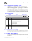
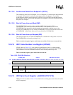
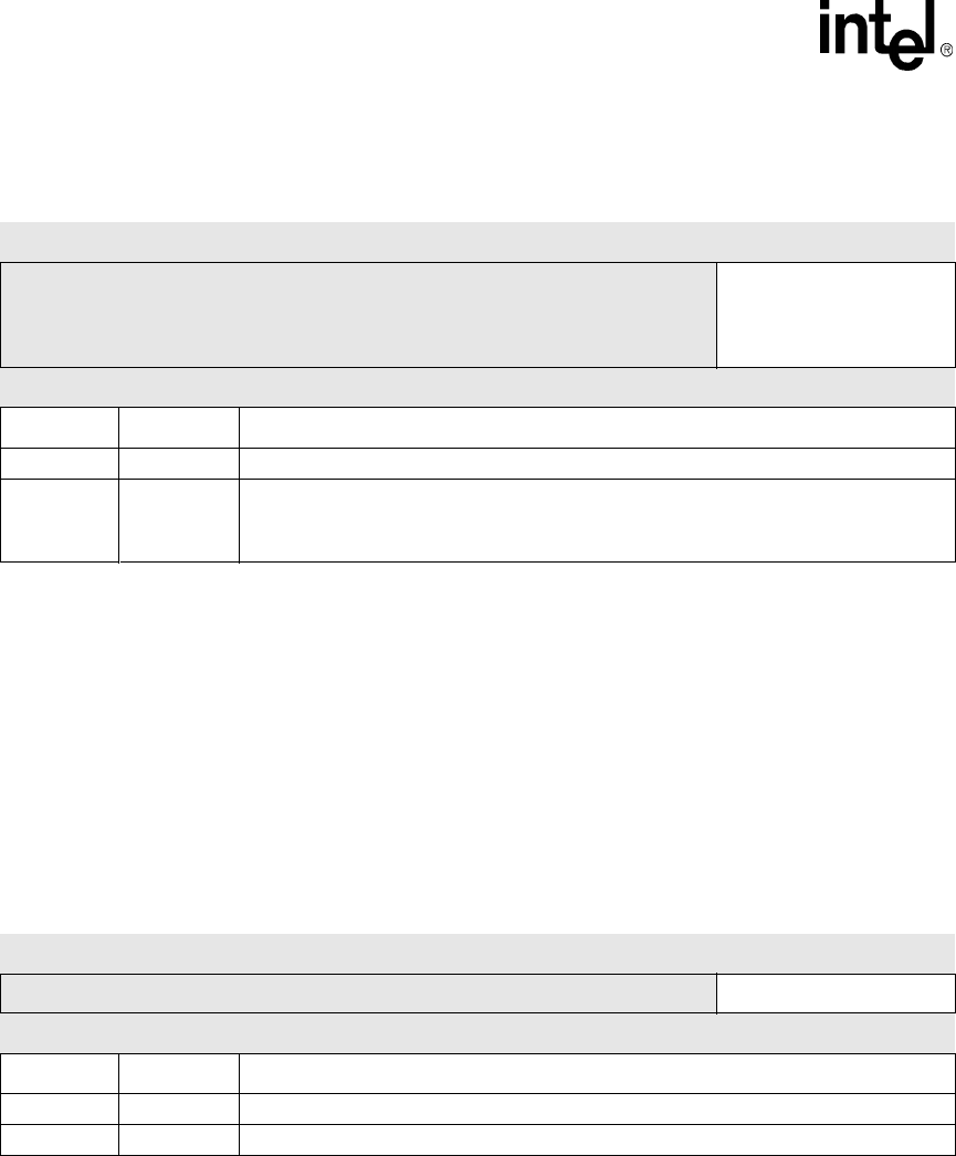
Table 12-28. UDDR1/6/11 Bit Definitions
0x 4060_0100
0x 4060_0600
0x 4060_0B00
UDDR1
UDDR6
UDDR11
USB Device Controller
Bit
31 30 29 28 27 26 25 24 23 22 21 20 19 18 17 16 15 14 13 12 11 10 9 8 7 6 5 4 3 2 1 0
reserved 8-Bit Data
Reset
x x x x x x x x x x x x x x x x x x x x x x x x x x 0 0 0 0 0 0
Bits Name Description
31:8 — reserved
7:0 DATA Top of endpoint data currently being loaded