


Intel® PXA255 Processor Developer’s Manual 2-11
System Architecture
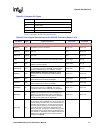
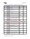
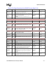
nPIOW/
GPIO[51]
ICOCZ
PCMCIA I/O write. (output) Performs write transactions
to PCMCIA I/O space.
Pulled High -
Note[1]
Note [5]
nPIOR/
GPIO[50]
ICOCZ
PCMCIA I/O read. (output) Performs read transactions
from PCMCIA I/O space.
Pulled High -
Note[1]
Note [5]
nPCE[2]/
GPIO[53]
ICOCZ
PCMCIA card enable 2. (output) Selects a PCMCIA
card. nPCE[2] enables the high byte lane and nPCE[1]
enables the low byte lane.
MMC clock. (output) Clock signal for the MMC
Controller.
Pulled High -
Note[1]
Note [5]
nPCE[1]/
GPIO[52]
ICOCZ
PCMCIA card enable 1. (outputs) Selects a PCMCIA
card. nPCE[2] enables the high byte lane and nPCE[1]
enables the low byte lane.
Pulled High -
Note[1]
Note [5]
nIOIS16/
GPIO[57]
ICOCZ
IO Select 16. (input) Acknowledge from the PCMCIA
card that the current address is a valid 16 bit wide I/O
address.
Pulled High -
Note[1]
Note [5]
nPWAIT/
GPIO[56]
ICOCZ
PCMCIA wait. (input) Driven low by the PCMCIA card to
extend the length of the transfers to/from the PXA255
processor.
Pulled High -
Note[1]
Note [5]
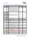
PSKTSEL/
GPIO[54]
ICOCZ
PCMCIA socket select. (output) Used by external
steering logic to route control, address, and data signals
to one of the two PCMCIA sockets. When PSKTSEL is
low, socket zero is selected. When PSKTSEL is high,
socket one is selected. Has the same timing as the
address bus.
Pulled High -
Note[1]
Note [5]
nPREG/
GPIO[55]
ICOCZ
PCMCIA Register select. (output) Indicates that the
target address on a memory transaction is attribute
space. Has the same timing as the address bus.
Pulled High -
Note[1]
Note [5]
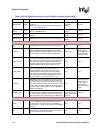
LCD Controller Pins
L_DD(7:0)/
GPIO[65:58]
ICOCZ
LCD display data. (outputs) Transfers pixel information
from the LCD Controller to the external LCD panel.
Pulled High -
Note[1]
Note [3]
L_DD[8]/
GPIO[66]
ICOCZ
LCD display data. (output) Transfers pixel information
from the LCD Controller to the external LCD panel.
Memory Controller alternate bus master request.
(input) Allows an external device to request the system
bus from the Memory Controller.
Pulled High -
Note[1]
Note [3]
L_DD[9]/
GPIO[67]
ICOCZ
LCD display data. (output) Transfers pixel information
from the LCD Controller to the external LCD panel.
MMC chip select 0. (output) Chip select 0 for the MMC
Controller.
Pulled High -
Note[1]
Note [3]
L_DD[10]/
GPIO[68]
ICOCZ
LCD display data. (output) Transfers pixel information
from the LCD Controller to the external LCD panel.
MMC chip select 1. (output) Chip select 1 for the MMC
Controller.
Pulled High -
Note[1]
Note [3]
L_DD[11]/
GPIO[69]
ICOCZ
LCD display data. (output) Transfers pixel information
from the LCD Controller to the external LCD panel.
MMC clock. (output) Clock for the MMC Controller.
Pulled High -
Note[1]
Note [3]
L_DD[12]/
GPIO[70]
ICOCZ
LCD display data. (output) Transfers pixel information
from the LCD Controller to the external LCD panel.
RTC clock. (output) Real time clock 1 Hz tick.
Pulled High -
Note[1]
Note [3]
Table 2-6. Pin & Signal Descriptions for the PXA255 Processor (Sheet 3 of 9)
Pin Name Type Signal Descriptions Reset State Sleep State