7-18 Intel® PXA255 Processor Developer’s Manual
LCD Controller
The DMA descriptor addresses are initially programmed by software. After that, the other DMA
registers are programmed by the hardware. Section 7.6.5 provides a complete description of how
the DMA is programmed.
The status registers contain bits that signal:
• Input and output FIFO overrun and underrun errors
• DMA bus errors
• When the DMAC starts and ends a frame
• When the last active frame has completed after the LCD is disabled
• Each time the L_BIAS pin has toggled a programmed number of times
Each of these hardware-detected events can signal an interrupt request to the interrupt controller.
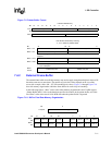
7.6.1 LCD Controller Control Register 0 (LCCR0)
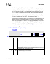
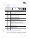
The control bits in LCCR0, shown in Table 7-3, within all other control registers must be
programmed before setting ENB=1 (a word write can be used to configure LCCR0 while setting
ENB after all other control registers have been programmed). The LCD controller must be disabled
when changing the state of any control bit within the LCD controller.
LCD Output Fifo Underrun Mask (OUM) — used to mask interrupt requests that are asserted
whenever an output FIFO underrun error occurs. When OUM=0, underrun interrupts are enabled,
and whenever an output FIFO underrun (OU) status bit within the LCD status register (LCSR) is
set (one), an interrupt request is made to the interrupt controller. When OUM=1, underrun
interrupts are masked and the state of the underrun status bit (OU) is ignored by the interrupt
controller. Setting OUM does not affect the current state of the status bit or the LCD controller’s
ability to set and clear it, it only blocks the generation of the interrupt request. Output FIFO
underruns are more critical than Input FIFO underruns, since Output FIFO underruns will affect the
display.
Branch Mask (BM) — used to mask interrupt requests that are asserted after the LCD Controller
has branched to a new set of frame descriptors. See Section 7.6.6 for details.
Palette DMA Request Delay (PDD) — used to select the minimum number of internal bus clock
cycles to wait between the servicing of each DMA request issued while the on-chip palette is
loaded. When the palette is optionally loaded at the beginning of a frame, up to 512 bytes of data
may be accessed by the LCD’s DMAC. Using PDD allows other bus masters to gain access to
shared memory in between palette DMA loads. PDD must be used carefully, as it can severely
degrade LCD controller performance if not used properly. It is recommended to leave PDD zero
and add delay only when necessary. PDD does not apply to the normal input FIFO DMA requests
for frame buffer information, since these DMA requests do not occur back-to-back. The input FIFO
DMA request rate is a function of the rate at which pixels are displayed on the screen.
After a word of palette data is written to the input FIFO, the value contained within PDD is loaded
to a down counter that disables the palette from issuing another DMA request until the counter
decrements to zero. This counter ensures that the LCD’s DMAC does not tie up the full bandwidth
of the processor system bus. Once the counter reaches zero, any pending or future DMA requests
by the palette cause the DMAC to arbitrate for the bus. Once the DMA burst cycle has completed,
the process starts over, and the value in PDD is loaded to the counter to create another wait state
period, which disables the palette from issuing a DMA request. PDD can be programmed with a


