


6-32 Intel® PXA255 Processor Developer’s Manual
Memory Controller
6.6 Synchronous Static Memory Interface
The synchronous static memory interface supports SMROM and non-SDRAM-like Flash
memories. The synchronous static memory can be configured for any of the nCS[3:0] signals. Chip
Select 0 must be used for boot memory. Synchronous static memories in bank pairs 1/0 or 3/2 must
be set to the same timing.
If any of the nCS[3:0] banks are configured for Synchronous Static Memory via
SXCNFG[SXENx], the corresponding half-words of MSC0 (see Section 6.7.3) and MSC1, except
the data width in MSCx[RBWx], are ignored.
6.6.1 Synchronous Static Memory Configuration Register
(SXCNFG)
SXCNFG controls all synchronous static memory. SXCNFG[15:0] configures chip select signals 0
and 1. SXCNFG[31:16] configures chip select signals 2 and 3.
This is a read/write register. Ignore reads from reserved bits. Write zeros to reserved bits.
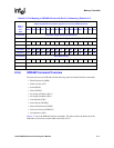
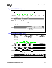
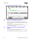
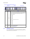
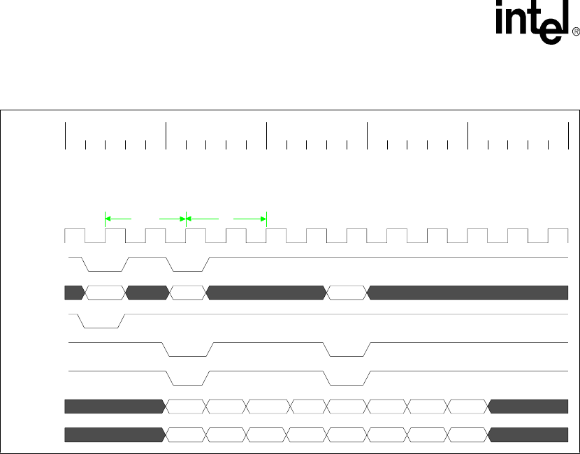
Figure 6-11. SDRAM 4-Beat Write / 4-Write Same Bank, Same Row
CLtRCD CLtRCD
row col
0123
mask0 mask1 mask3mask2
tRP = 2 clks
tRCD = 2 clks
tRAS = 2 clks
CL = 2 clks
col
4567
mask4 mask5 mask6 mask7
0ns 25ns 50ns 75ns 100ns
SDCLK
nSDCS
MA[24:0]
nSDRAS
nSDCAS
nWE
DATA
DQM[3:0]