


4-6 Intel® PXA255 Processor Developer’s Manual
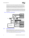
System Integration Unit
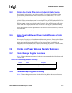
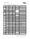
4.1.3 GPIO Register Definitions
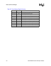
There are twenty-seven 32-bit registers within the GPIO control block. There are nine distinct
register functions and there are three sets of each of the nine registers to serve the 85 GPIOs. The
various functions of the nine registers corresponding to each GPIO pin are described here:
• Three monitor pin state (GPLR)
• Six control output pin state (GPSR, GPCR)
• Three control pin direction (GPDR)
• Six control whether rising edges and/or falling edges are detected (GRER & GFER)
• Three indicate when specified edge types have been detected on pins (GEDR).
• Six determine whether a pin is used as a normal GPIO or whether it is to be taken over by one
of three possible alternate functions (GAFR_L, GAFR_U).
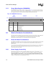
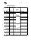
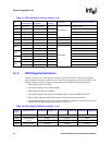
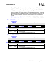
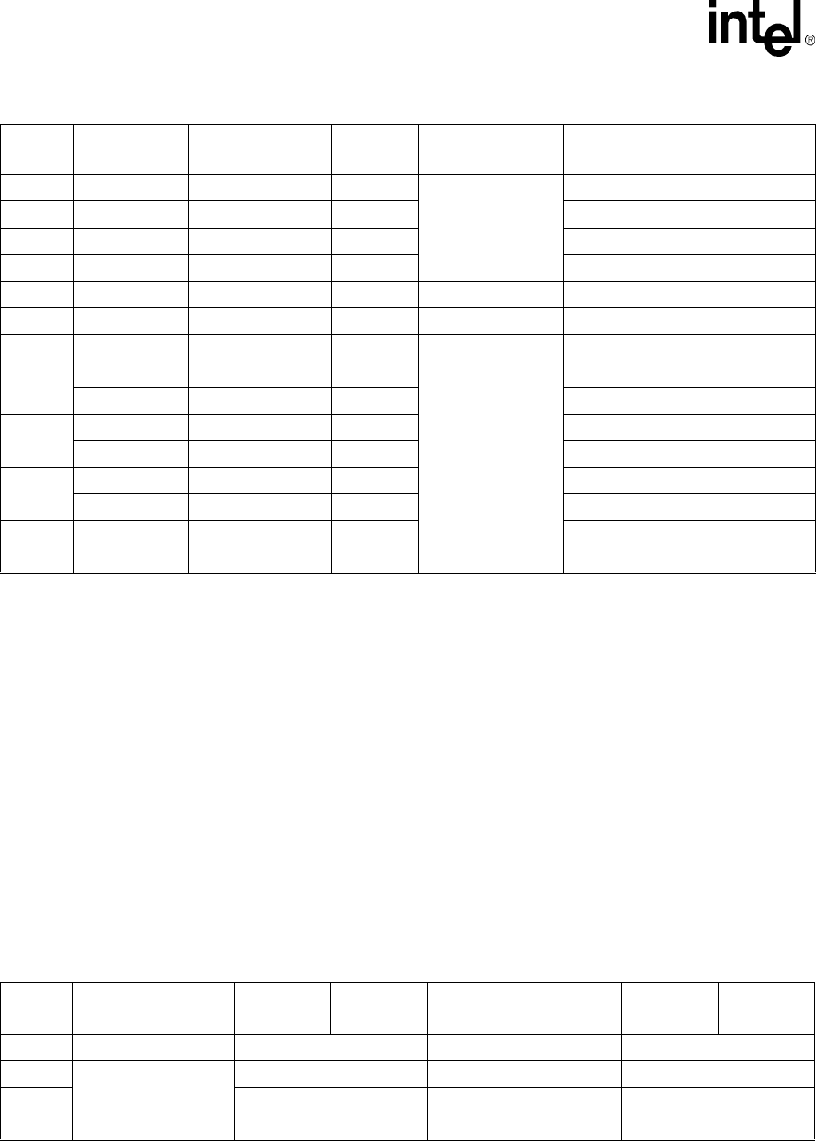
GP74 LCD_FCLK ALT_FN_2_OUT 10
LCD Controller
LCD Frame clock
GP75
LCD_LCLK ALT_FN_2_OUT 10 LCD line clock
GP76
LCD_PCLK ALT_FN_2_OUT 10 LCD Pixel clock
GP77
LCD_ACBIAS ALT_FN_2_OUT 10 LCD AC Bias
GP78
nCS[2] ALT_FN_2_OUT 10 Memory Controller Active low chip select 2
GP79
nCS[3] ALT_FN_2_OUT 10 Memory Controller Active low chip select 3
GP80
nCS[4] ALT_FN_2_OUT 10 Memory Controller Active low chip select 4
GP81
NSSPSCLK ALT_FN_1_IN 01
Network SSP
NSSP Serial clock is input
NSSPSCLK ALT_FN_1_OUT 01 NSSP Serial clock is output
GP82
NSSPSFRM ALT_FN_1_IN 01 NSSP frame is input
NSSPSFRM ALT_FN_1_OUT 01 NSSP frame is output
GP83
NSSPTXD ALT_FN_1_OUT 01 NSSP transmit
NSSPRXD ALT_FN_2_IN 10 NSSP receive
GP84
NSSPTXD ALT_FN_1_OUT 01 NSSP transmit
NSSPRXD ALT_FN_2_IN 10 NSSP receive
† CKEN[11] - USB Unit Clock Enable bit must be enabled to allow the 48 MHz clock output on GP7
Table 4-1. GPIO Alternate Functions (Sheet 4 of 4)
Pin
Alternate
Function Name
Alternate Function
Assignment
AF{n}
encoding
Source Unit Signal Description and comments
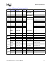
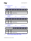
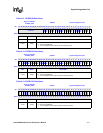
Table 4-2. GPIO Register Definitions (Sheet 1 of 2)
Register
Type
Register Function GPIO[15:0] GPIO[31:16] GPIO[47:32] GPIO[63:48] GPIO[79:64] GPIO[80:84]
GPLR Monitor Pin State GPLR0 GPLR1 GPLR2
GPSR
Control Output
Pin State
GPSR0 GPSR1 GPSR2
GPCR GPCR0 GPCR1 GPCR2
GPDR Set Pin Direction GPDR0 GPDR1 GPDR2