


7-24 Intel® PXA255 Processor Developer’s Manual
LCD Controller
7.6.2 LCD Controller Control Register 1 (LCCR1)
LCCR1, shown in Table 7-4, contains four bit fields that are used as modulus values for a
collection of down counters, each of which performs a different function to control the timing of
several of the LCD pins. These values must be programmed before enabling the LCD Controller.
9DPD
Double-Pixel Data (DPD) pin mode:
In passive monochrome single panel mode,
0 = L_DD[3:0] pins are used to send 4 pixel values each pixel clock transition.
1 = L_DD[7:0] pins are used to send 8 pixel values each pixel clock.
In any other mode, DPD must be 0.
8 — reserved
7PAS
Passive/Active Display select:
0 = Passive (or STN) display operation enabled.
1 = Active (or TFT) display operation enabled.
6EFM
End of Frame Mask:
0 = Generates an interrupt at the end of a frame.
1 = End of frame (EOF) condition does not generate an interrupt.
5IUM
Input FIFO Underrun Mask:
0 = FIFO underrun errors generate an interrupt.
1 = FIFO underrun errors do not generate an interrupt.
4SFM
Start of Frame Mask:
0 = Starting a new frame (after loading frame descriptor) generates an interrupt.
1 = Start of frame (SOF) condition does not generate an interrupt.
3LDM
LCD Disable Done Mask:
0 = LCD disable done condition generates an interrupt (state of LDD status sent to the
interrupt controller).
1 = LCD disable done condition does not generate an interrupt (LDD status bit ignored).
2SDS
Single-/Dual-panel Display Select:
0 = Single-panel display enabled.
1 = Dual-panel display enabled.
SDS must be 0 in active mode (PAS=1).
1CMS
Color/Monochrome Select:
0 = Color operation enabled.
1 = Monochrome operation enabled.
0ENB
LCD Controller Enable:
0 = LCD controller disabled or in the process of quickly disabling.
1 = LCD controller enabled.
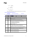
Table 7-3. LCCR0 Bit Definitions (Sheet 2 of 2)
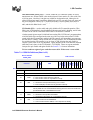
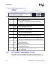
Physical Address
0x4400_0000
LCCR0 LCD Controller
Bit
31 30 29 28 27 26 25 24 23 22 21 20 19 18 17 16 15 14 13 12 11 10 9 8 7 6 5 4 3 2 1 0
reserved
OUM
BM
PDD
QDM
DIS
DPD
reserved
PAS
EFM
IUM
SFM
LDM
SDS
CMS
ENB
Reset X X X X X X X X X X X X 0 0 0 0 0 0 0 0 0 0 0 0 0 0 0 0 0 0 0 0
Bits Name Description