


7-8 Intel® PXA255 Processor Developer’s Manual
LCD Controller
7.3.4 Output FIFOs
The LCD controller has two output FIFOs to queue pixel data before it is sent out to the pins. Each
output FIFO is 16 bytes, organized as 16 entries by 8 bits wide. Pixel values are accumulated in a
serial shifter and written to the FIFO buffers in 4-, 8-, or 16-bit quantities. Four pins are used for
single-panel monochrome screens, 8 pins are used for single- and dual-panel monochrome screens
and single-panel color displays, and 16 pins are used for dual-panel color and active displays. Each
time a value is taken from the bottom of the FIFO, the entry is invalidated, and all data in the FIFO
moves down one position.
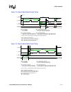
7.3.5 LCD Controller Pin Usage
The timing of the line (L_LCLK) and frame (L_FCLK) clocks is programmable to support both
passive display and active display modes. Programming options include: wait state insertion at the
beginning and end of each line and frame, pixel clock (L_PCLK), line clock, frame clock
(L_FCLK), output enable signal polarity, and frame clock pulse width.
See Section 7.5 for pin timing diagrams. When the LCD controller is disabled, all of its pins can be
used for GPIO. See Chapter 4, “System Integration Unit” for further details. See also Table 7-1.
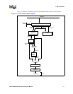
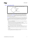
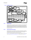
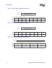
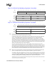
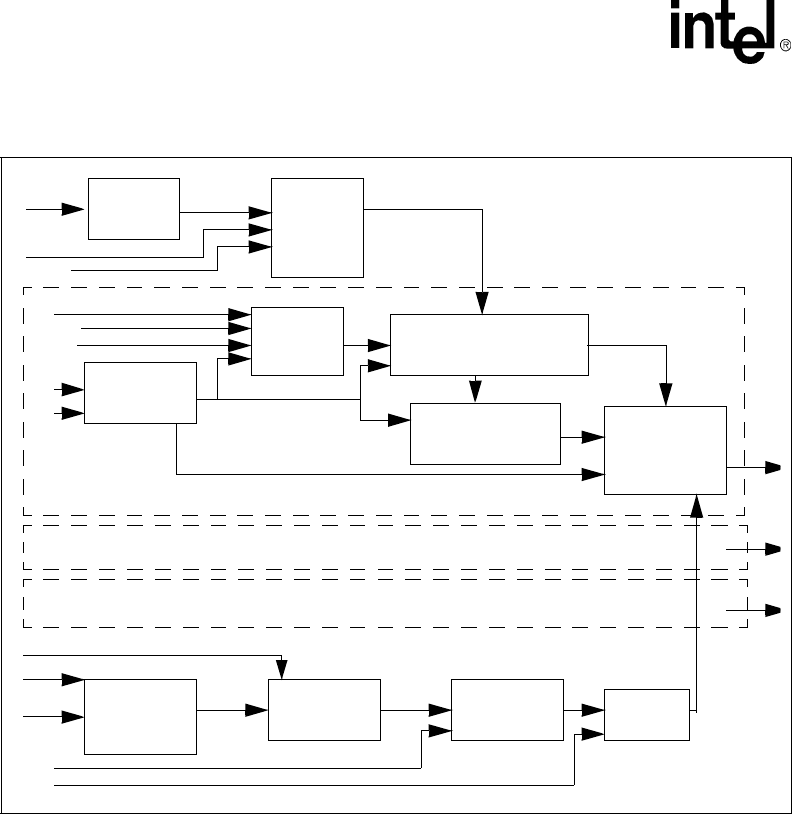
Figure 7-4. TMED Block Diagram
Lower Boundary
LB =FN x CV + Offset
Generator
Frame
Counter
Upper Boundary
UB =LB + CV
Generator
Color Value
Generator
Color
Offset
Adjuster
Data
Generator
LB > ME > UB
or Pixel > 253
Single Color Component Path (GREEN)
Single Color Component Path (BLUE)
Single Color Component Path (RED)
Outpu
Data
Bit
Frame
Number
Adjuster
FN
CV
LB
UB
LB
Outpu
Data
Bit
Outpu
Data
Bit
Line Counter
Pixel Number
Adjustor
Address
Generator
Matrix
Pixel Counter
frame_clk
line clk
pixel clk
TCR is the TMED Control Register
TCR<13:12>
pixel
data
TCR<1>
TCR<0>
TCR<2>
TSR is the TMED Seed Register
TSR<7:0>
TCR<3>
TCR<14>
TCR<11:8>
TCR<7:4>
force to 1
ME