


Intel® PXA255 Processor Developer’s Manual 6-79
Memory Controller
In sleep mode, the memory pins and controller are in the same state as they are after a hardware
reset, except that the GPIO signals are driven high. If SDRAMs are in self-refresh, they are held
there by setting SDCKE<1> to a 0.
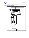
6.11 Hardware, Watchdog, or Sleep Reset Operation
Software performs the following procedures when the processor comes out of a reset:
1. After hardware reset, complete a power-on wait period of 200 µs, which allows the internal
clocks that generate SDCLK to stabilize. Enable MDREFR:K0RUN and E0PIN for
Synchronous Static memory. When MDREFR is written, a refresh interval value
(MDREFR:DRI) must also be written. The following writes are allowed:
a. Write MSC0, MSC1, MSC2
b. Write MECR, MCMEM0, MCMEM1, MCATT0, MCATT1, MCIO0, MCIO1
c. Write MDREFR:K0RUN and MDREFR:E0PIN. Configure MDREFR:K0DB2. Retain
the current values of MDREFR:APD and MDREFR:SLFRSH. MDREFR:DRI must
contain a valid value. Deassert MDREFR:KxFREE.
2. In systems that contain Synchronous Static memory, write to the SXCNFG to configure all
appropriate bits, including the enable bits. Software must perform a sequence that involves a
subsequent write to SXCNFG to change the RAS latencies. While any SMROM banks are
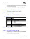
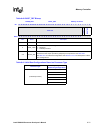
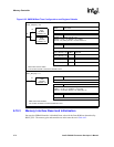
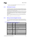
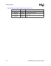
Table 6-42. Memory Controller Pin Reset Values
Pin Name PXA255 Processor Reset Value
SDCLK [2:0] 000
SDCKE <1> 00
SDCKE <0> 1 if BOOT_SEL = Synchronous Memory
DQM [3:0] 0000
nSDCS [3:0] 1111
nWE 1
nSDRAS 1
nSDCAS 1
nOE 1
MA [25:0] 0x0000000h
RDnWR 0
MD [31:0] 0x00000000h
nCS <0> 1
nCS <5:1> GPIO Input
nPIOIR GPIO Input
nPIOIW GPIO Input
nPOE GPIO Input
nPWE GPIO Input