


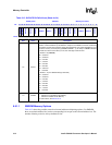
6-36 Intel® PXA255 Processor Developer’s Manual
Memory Controller
6.6.1.1 SMROM Memory Options
Table 6-15 shows the possible external-to-internal address multiplexing options. For SMROM,
there are no bank-address bits, but the corresponding bits are put on the external address bus. The
number of banks per device always defaults to four.
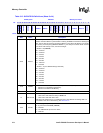
4:2 SXCL0
CAS Latency for SX Memory partition pair 0/1
Number of external SDCLK cycles between reception of the READ command and latching
of the data. The unit size for SXCL0 is the external SDCLK cycle. When SX Memory is run
at half the memory clock frequency (MDREFR:K0DB2 = 1), the delay is 2*MEMCLK When
in doubt as to which CAS Latency to use, the next larger must be used.
IF SXTP0 = 00 (SMROM):
000 – reserved
001 – reserved
010 – 3 clocks
011 – 4 clocks
100 – 5 clocks
101 – 6 clocks
110 – reserved
111 – reserved
IF SXTP0 = 10 (non-SDRAM timing Fast Flash)
000 – reserved
001 – reserved
010 – 3 clocks
011 – 4 clocks
100 – 5 clocks
101 – 6 clocks
110 – 7 clocks
111 – reserved
1:0 SXEN0
Enable Bits for SX Memory Partition 0 (bit 0) and Partition 1 (bit 1)
0 – Partition is not enabled as SX Memory
1 – Partition is enabled as SX Memory
For reset values, see Section 6.10.
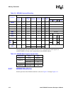
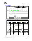
Table 6-13. SXCNFG Bit Definitions (Sheet 4 of 4)
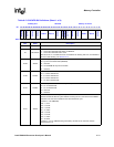
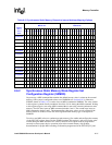
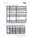
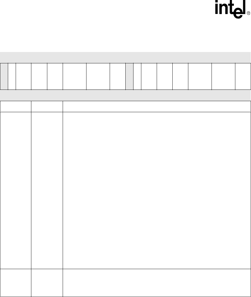
0x4800_001C SXCNFG Memory Controller
Bit
31 30 29 28 27 26 25 24 23 22 21 20 19 18 17 16 15 14 13 12 11 10 9 8 7 6 5 4 3 2 1 0
reserved
SXLATCH2
SXTP2
SXCA2
SXRA2
SXRL2 SXCL2
SXEN2
reserved
SXLATCH0
SXTP0
SXCA0
SXRA0
SXRL0 SXCL0
SXEN0
Reset 0 0 0 0 0 0 0 0 0 0 0 0 0 0 0 0 0 * * * * * * * * * * * * * 0 *
Bits Name Description