


Intel® PXA255 Processor Developer’s Manual 3-25
Clocks and Power Manager
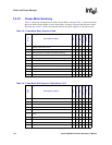
3.5.3 Power Manager Wake-Up Enable Register (PWER)
Table 3-9 shows the location of all wake up source enable bits in the Power Manager Wake-Up
Enable Register (PWER). If a GPIO is to be used as a wake up source from Sleep, it must be
programmed as an input in the GPDR and either one or both of the corresponding bits in the PRER
and PFER must be set. When the IDAE bit is zero and a fault condition is detected on the
nVDD_FAULT or nBATT_FAULT pin, PWER is set to 0x0000 0003 and only allows GP[1:0] as
wake-up sources. When the IDAE bit is set, fault conditions on the nVDD_FAULT or
nBATT_FAULT pins do not affect wake-up sources. PWER is also set to 0x0000 0003 in
Hardware, Watchdog, or GPIO Resets.
Software should enable wakeups only for those GPIO pins that are configured as inputs during
sleep. Any GPIO pins that are configured as outputs during sleep, should have their associated
wake enable bits set to logic zero in all three PMU wake enable registers (PWER, PRER, and
PFER).
This is a read/write register. Ignore reads from reserved bits. Write zeros to reserved bits.
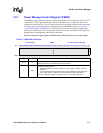
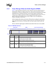
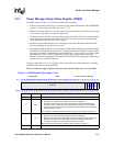
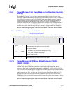
Table 3-9. PWER Bit Definitions
0x40F0_000C PWER Clocks and Power Manager
Bit
31 30 29 28 27 26 25 24 23 22 21 20 19 18 17 16 15 14 13 12 11 10 9 8 7 6 5 4 3 2 1 0
WERTC
Reserved
WE15
WE14
WE13
WE12
WE11
WE10
WE9
WE8
WE7
WE6
WE5
WE4
WE3
WE2
WE1
WE0
Reset 0 0 0 0 0 0 0 0 0 0 0 0 0 0 0 0 0 0 0 0 0 0 0 0 0 0 0 0 0 0 1 1
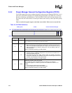
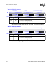
Bits Name Description
31 WERTC
RTC Sleep Mode Wake-up Enable.
0 – Wake-up due to RTC alarm disabled.
1 – Wake-up due to RTC alarm enabled.
Cleared on hardware, watchdog, and GPIO resets.
[30:16] —
Reserved.
Read undefined and must always be written with zeroes.
[15:0] WEx
Sleep Mode Wake-up Enable
0 – Wake-up due to GPx edge detect disabled.
1 – Wake-up due to GPx edge detect enabled.
Set to 0x 0003 on hardware, watchdog, and GPIO resets.