Intel® PXA255 Processor Developer’s Manual 6-47
Memory Controller
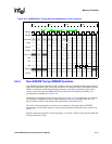
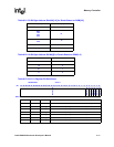
Table 6-24. MSC0/1/2 Bit Definitions (Sheet 1 of 3)
0x4800_0008
0x4800_000C
0x4800_0010
MSC0
MSC1
MSC2
Memory Controller
Bit
31 30 29 28 27 26 25 24 23 22 21 20 19 18 17 16 15 14 13 12 11 10 9 8 7 6 5 4 3 2 1 0
RBUFF1/3/5
RRR1/3/5 RDN1/3/5 RDF1/3/5
RBW1/3/5
RT1/3/5
RBUFF0/2/4
RRR0/2/4
RDN0/2/4 RDF0/2/4
RBW0/2/4
RT0/2/4
Reset
0 1 1 1 1 1 1 1 1 1 1 1 0 0 0 0 0 1 1 1 1 1 1 1 1 1 1 1 * 0 0 0
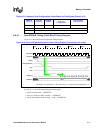
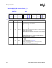
Bits Access Name Description
15 R/W RBUFFx
Return Data Buffer vs. Streaming behavior.
When slower memory devices are being used in the system (e.g. VLIO,
slow SRAM/ROM), this bit must be reset to allow the system to not have to
remain idle while all data is being read from the device. By resetting this bit,
the system is allowed to process other information. When set, the internal
bus may halt while all data is returned from the device. The value of the
RBUFF bit does not affect the behavior of the external memory bus. Once a
transaction begins on the memory bus, it must be completed before another
transaction starts.
When Synchronous Static memory devices have been enabled for a given
bank, this value will default to Streaming behavior (assuming a faster
device). The register bit will still read as 0 (Return Data Buffer) unless it has
specifically been programmed to a 1. This cannot be overridden.
0 – Slower device (Return Data Buffer)
1 – Faster device (Streaming behavior)
14:12 R/W RRRx<2:0>
ROM/SRAM recovery time.
Chip select deasserted after a read/write to next chip select (including the
same static memory bank) or nSDCS asserted is equal to (RRRx * 2)
memclks.
This field must be programmed with the maximum of t
OFF
(divided by 2),
write pulse high time (Flash/SRAM), and write recovery before read (Flash).
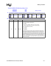
11:8 R/W RDNx<3:0>
ROM delay next access
Address to data valid for subsequent access to burst ROM or Flash is equal
to (RDNx + 1) memclks.
nWE assertion for write accesses to SRAM is equal to (RDFx + 1) memclks.
The nOE (nPWE) deassert time between each beat of read/write for
Variable Latency I/O is equal to (RDNx + 2) memclks. For variable latency
I/O, this number must be greater than or equal to 2.


