


Intel® PXA255 Processor Developer’s Manual 6-27
Memory Controller
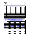
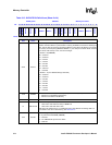
6.5.6 SDRAM Command Overview
The processor accesses SDRAM with the following subset of standard interface commands:
• Mode Register Set (MRS)
• Bank Activate (ACT)
• Read (READ)
• Write (WRITE)
• Pre-charge All Banks (PALL)
• Pre-charge One Bank (PRE)
• Auto-Refresh (CBR)
• Power-Down (PWRDN)
• Enter Self-Refresh (SLFRSH)
• Exit Power-Down (PWRDNX)
• No Operation (NOP)
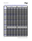
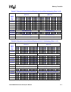
Table 6-11 shows the SDRAM interface commands. The table assumes the bank bits for the
SDRAM are sent out on external address lines MA<24:23>.
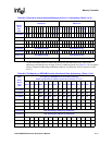
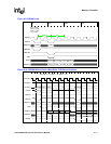
2x12x11x32 NOT VALID (illegal addressing combination)
2x12x11x16 NOT VALID (illegal addressing combination)
2x13x8x32 A12 BA1 BA0 A11 A10 A9 A8 A7 A6 A5 A4 A3 A2 A1 A0
2x13x8x16 NOT VALID (illegal addressing combination)
2x13x9x32 A12 BA1 BA0 A11 A10 A9 A8 A7 A6 A5 A4 A3 A2 A1 A0
2x13x9x16 A12 BA1 BA0 A11 A10 A9 A8 A7 A6 A5 A4 A3 A2 A1 A0
2x13x10x32 NOT VALID (too big)
2x13x10x16A12BA1BA0A11A10A9A8A7A6A5A4A3A2A1A0
2x13x11x32 NOT VALID (too big)
2x13x11x16 NOT VALID (too big)
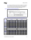
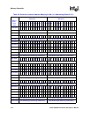
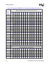
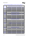
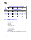
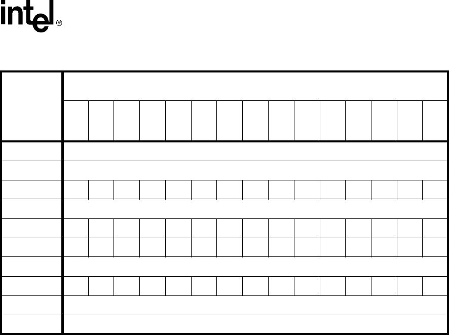
Table 6-10. Pin Mapping to SDRAM Devices with SA1111 Addressing (Sheet 3 of 3)
# Bits
Bank x
Row x
Col x
Data
Pin mapping to SDRAM devices for SA1111 Addressing Options.
MA[24:10] represent the address signals driven from the PXA255 processor.
MA24 MA23 MA22 MA21 MA20 MA19 MA18 MA17 MA16 MA15 MA14 MA13 MA12 MA11 MA10