


Intel® PXA255 Processor Developer’s Manual 2-17
System Architecture
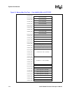
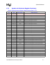
TDO OCZ
JTAG test data output. (output) Data from the PXA255
processor is returned to the JTAG controller using this
pin.
Hi-Z Hi-Z
TMS IC
JTAG test mode select. (input) Selects the test mode
required from the JTAG controller. This pin has an
internal pull-up resistor.
Input Input
TCK IC
JTAG test clock. (input) Clock for all transfers on the
JTAG test interface.
Input Input
TEST IC Test Mode. (input) Reserved. Must be grounded. Input Input
TESTCLK IC Test Clock. (input) Reserved. Must be grounded. Input Input
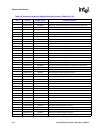
Power and Ground Pins
VCC SUP
Positive supply for internal logic. Must be connected
to the low voltage supply on the PCB.
Powered Note [6]
VSS SUP
Ground supply for internal logic. Must be connected to
the common ground plane on the PCB.
Grounded Grounded
PLL_VCC SUP
Positive supply for PLLs and oscillators. Must be
connected to the common low voltage supply.
Powered Note [6]
PLL_VSS SUP
Ground supply for the PLL. Must be connected to
common ground plane on the PCB.
Grounded Grounded
VCCQ SUP
Positive supply for all CMOS I/O except memory bus
and PCMCIA pins. Must be connected to the common
3.3v supply on the PCB.
Powered Note [7]
VSSQ SUP
Ground supply for all CMOS I/O except memory bus
and PCMCIA pins. Must be connected to the common
ground plane on the PCB.
Grounded Grounded
VCCN SUP
Positive supply for memory bus and PCMCIA pins.
Must be connected to the common 3.3v or 2.5v supply on
the PCB.
Powered Note [7]
VSSN SUP
Ground supply for memory bus and PCMCIA pins.
Must be connected to the common ground plane on the
PCB.
Grounded Grounded
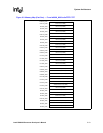
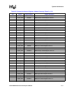
Table 2-7. Pin Description Notes (Sheet 1 of 2)
Note Description
[1]
GPIO Reset Operation: Configured as GPIO inputs by default after any reset. The input buffers for these pins
are disabled to prevent current drain and the pins are pulled high with 10K to 60K internal resistors. The input
paths must be enabled and the pullups turned off by clearing the Read Disable Hold (RDH) bit described in
Section 3.5.7, “Power Manager Sleep Status Register (PSSR)” on page 3-29. Even though sleep mode sets the
RDH bit, the pull-up resistors are not re-enabled by sleep mode.
[2]
Crystal oscillator pins: These pins are used to connect the external crystals to the on-chip oscillators. Refer to
Section 3.3.1, “32.768 kHz Oscillator” on page 3-4 and Section 3.3.2, “3.6864 MHz Oscillator” on page 3-4 for
details on Sleep Mode operation.
[3]
GPIO Sleep operation: During the transition into sleep mode, the state of these pins is determined by the
corresponding PGSRn. See Section 3.5.10, “Power Manager GPIO Sleep State Registers (PGSR0, PGSR1,
PGSR2)” and Section 4.1.3.2, “GPIO Pin Direction Registers (GPDR0, GPDR1, GPDR2)” on page 4-8. If
selected as an input, this pin does not drive during sleep. If selected as an output, the value contained in the
Sleep State Register is driven out onto the pin and held there while the PXA255 processor is in Sleep Mode.
GPIOs configured as inputs after exiting sleep mode cannot be used until PSSR[RDH] is cleared.
Table 2-6. Pin & Signal Descriptions for the PXA255 Processor (Sheet 9 of 9)
Pin Name Type Signal Descriptions Reset State Sleep State