


Intel® PXA255 Processor Developer’s Manual 6-35
Memory Controller
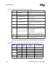
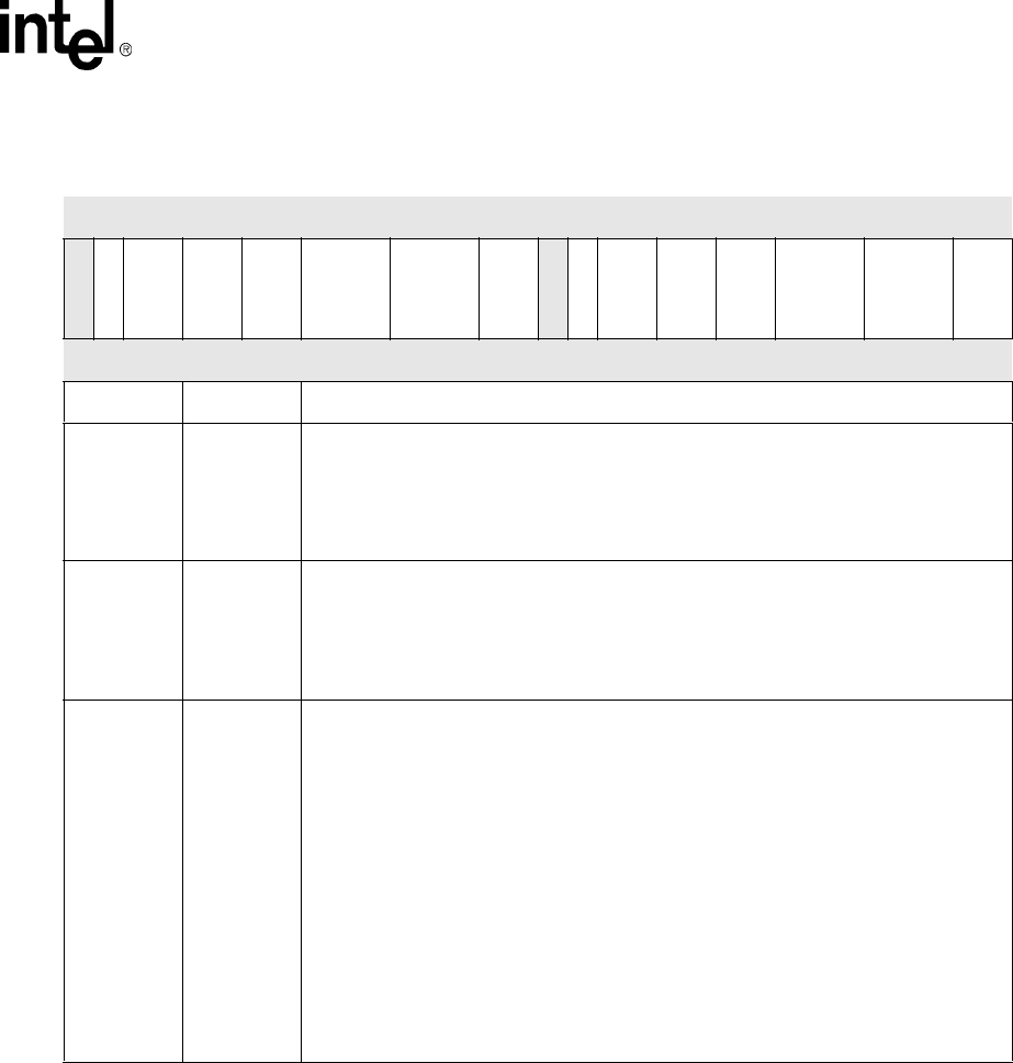
11:10 SXCA0
SX Memory column address bit count for partition pair 0/1
00 – 7 column address bits
01 – 8 column address bits
10 – 9 column address bits
11 – 10 column address bits
9:8 SXRA0
SX Memory row address bit count for partition pair 0/1
00 – 12 row address bits
01 – 13 row address bits
10 – reserved
11 – reserved
7:5 SXRL0
RAS Latency for Synchronous Static (SX) Memory partition pair 0/1
Number of external SDCLK cycles between reception of the ACT command and reception
of the READ command. The unit size for SXRL0 is the external SDCLK cycle.
IF SXTP0 = 00 (SMROM):
000 – 1 clock
001 – 2 clocks
010 – 3 clocks
011 – 4 clocks
100 – 5 clocks
101 – 6 clocks
110 – 7 clocks
111 – 8 clocks
IF SXTP0 = 10 (non-SDRAM timing Fast Flash), this field is not used and must be
programmed to 111
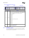
Table 6-13. SXCNFG Bit Definitions (Sheet 3 of 4)
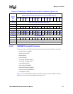
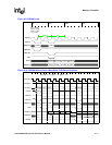
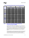
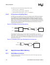
0x4800_001C SXCNFG Memory Controller
Bit
31 30 29 28 27 26 25 24 23 22 21 20 19 18 17 16 15 14 13 12 11 10 9 8 7 6 5 4 3 2 1 0
reserved
SXLATCH2
SXTP2
SXCA2
SXRA2
SXRL2 SXCL2
SXEN2
reserved
SXLATCH0
SXTP0
SXCA0
SXRA0
SXRL0 SXCL0
SXEN0
Reset 0 0 0 0 0 0 0 0 0 0 0 0 0 0 0 0 0 * * * * * * * * * * * * * 0 *
Bits Name Description