


Intel® PXA255 Processor Developer’s Manual 6-11
Memory Controller
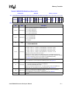
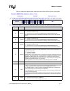
20:19 DCAC2[1:0]
Number of Column Address bits for partition pair 2/3
00 – 8 column address bits
01 – 9 column address bits
10 – 10 column address bits
11 – 11 column address bits
22:21 DRAC2[1:0]
SDRAM row address bit count for partition pair 2/3
00 – 11 row address bits
01 – 12 row address bits
10 – 13 row address bits
11 – reserved
23 DNB2
Number of banks in upper partition pair
0 – 2 internal SDRAM banks
1 – 4 internal SDRAM banks
25:24 DTC2[1:0]
Timing Category for SDRAM pair 2/3
00 – tRP = 2 clks, CL = 2, tRCD = 1 clks, tRAS(min) = 3 clks, tRC = 4 clks
01 – tRP = 2 clks, CL = 2, tRCD = 2 clks, tRAS(min) = 5 clks, tRC = 8 clks
10 – tRP = 3 clks, CL = 3, tRCD = 3 clks, tRAS(min) =7 clks, tRC=10 clks
11 – tRP = 3 clks, CL = 3, tRCD = 3 clks, tRAS(min) = 7 clks, tRC = 11 clks
tWR (write recovery time) is fixed at 2 clocks.
These bits are used to configure the SDRAM timings per the SDRAM manufacturer’s
specifications. Clocks referred to in the timings above are the number of SDCLKs. SDCLKs
may not be equivalent to memory clocks based on the MDREFRx[KxDB2].
See Figure 6-5 for a description of these timing numbers.
26 DADDR2
reserved
For an explanation on how the alternate addressing works, see Figure 6-4.
27 DLATCH2
Return Data from SDRAM latching scheme for pair 2/3
0 – Latch return data using fixed delay from MEMCLK
1 – Latch return data with return clock
This bit must always be written with a ‘1’ to enable using the return clock SDCLK for
latching data. For more detail on this return data latching, see Section 6.5.4.
28 DSA1111_2
Use SA1111 Addressing Muxing Mode for pair 2/3. Setting this bit will override the
addressing bit programmed in MDCNFG:DADDR2.
For an explanation on how the SA1111 addressing works, see Table 6-8.
31:29 — reserved
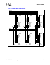
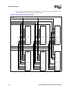
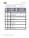
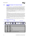
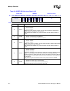
Table 6-2. MDCNFG Bit Definitions (Sheet 3 of 3)
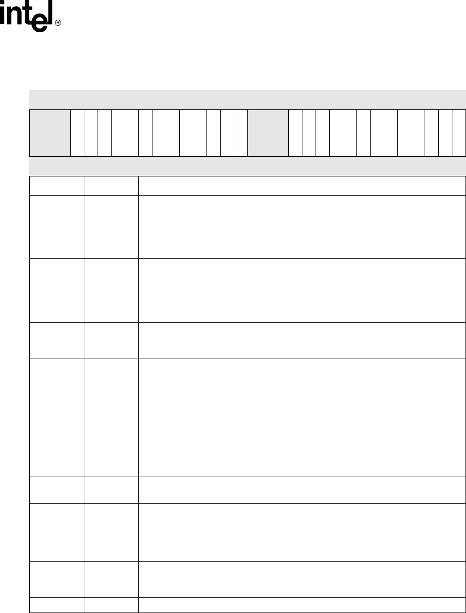
0x4800_0000 MDCNFG Memory Controller
Bit
31 30 29 28 27 26 25 24 23 22 21 20 19 18 17 16 15 14 13 12 11 10 9 8 7 6 5 4 3 2 1 0
reserved
DSA1111_2
DLATCH2
DADDR2
DTC2
DNB2
DRAC2
DCAC2
DWID2
DE3
DE2
reserved
DSA1111_0
DLATCH0
DADDR0
DTC0
DNB0
DRAC0
DCAC0
DWID0
DE1
DE0
Reset 0 0 0 0 0 0 0 0 0 0 0 0 0 0 0 0 0 0 0 0 0 0 0 0 0 0 0 0 0 0 0 0
Bits Name Description