


6-40 Intel® PXA255 Processor Developer’s Manual
Memory Controller
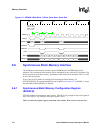
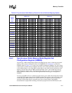
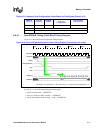
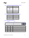
Table 6-18 shows sample frequency configurations for programming non-SDRAM Timing Fast
Flash. When in doubt, the higher frequency configuration and corresponding CAS latency must be
used.
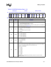
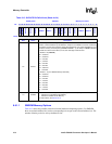
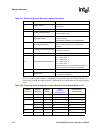
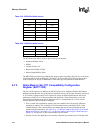
Table 6-17. Read Configuration Register Programming Values
Bits Field Name Value to Program
2:0 BURST LENGTH
010
8 Word Burst
5:3 reserved 000
6 CLOCK CONFIGURATION
1
Use rising edge of clock
7 BURST SEQUENCE
1
Linear burst Order
(INTEL BURST ORDER IS NOT SUPPORTED)
8 WAIT CONFIGURATION
N/A
nWAIT from the Flash device is ignored by the
processor.
9 DATA OUTPUT CONFIGURATION
0
Hold data for one clock
10 reserved 0
13:11 FREQUENCY CONFIGURATION
010 -> CAS Latency 3
011 -> CAS Latency 4
100 -> CAS Latency 5
101 -> CAS Latency 6
110 -> CAS Latency 7
Chosen based on the AC Characteristics - Read only
Operation section of the Flash device data sheet
14 reserved 0
15 READ MODE
0 - Synchronous Operation
1 - Asynchronous Operation
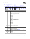
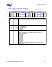
Table 6-18. Frequency Code Configuration Values Based on Clock Speed (Sheet 1 of 2)
MEMCLK
Frequency
SDCLK0
Frequency
MDREFR:
K0DB2
Valid
Frequency
Configurations
Corresponding
CAS Latencies
20 20 0 2 / 3 / 4 / 5 / 6 3 / 4 / 5 / 6 / 7
33 33 0 3 / 4 / 5 / 6 4 / 5 / 6 / 7
50
50 0 4 / 5 / 6 5 / 6 / 7
25 1 2 / 3 / 4 / 5 / 6 3 / 4 / 5 / 6 / 7
66
66 0 5 / 6 6 / 7
33 1 3 / 4 / 5 / 6 4 / 5 / 6 / 7
100 50 1 4 / 5 / 6 5 / 6 / 7
118 59 1 5 / 6 6 / 7