


Intel® PXA255 Processor Developer’s Manual 8-15
Synchronous Serial Port Controller
This is a read/write register. Ignore reads from reserved bits. Write zeros to reserved bits.
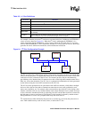
8.7.3 SSP Data Register (SSDR)
SSDR, shown in Table 8-5, is a single address location that can be accessed by read/write data
transfers. Transfers can be single transfers, 4 half-word bursts, or 8 half-word bursts.
As the system accesses the register, FIFO control logic transfers data automatically between
register and FIFO as fast as the system moves data. The SSP Status Register has bits that indicate
whether either FIFO is full, above/below a programmable threshold, or empty.
For transmit operations from SSPC to SSP peripheral, the CPU (using programmed I/O) may write
to the SSDR when the transmit FIFO is below its threshold level.
When a data size less than 16-bits is selected, do not left-justify data before it is written to the
SSDR. Transmit logic left-justifies the data and ignores any unused bits. Received data less than
16-bits is automatically right-justified in the receive FIFO.
When the SSPC is programmed for National Microwire frame format and the size for transmit data
is 8-bits, as selected by the MWDS bit in the SSCR1, the most significant byte is ignored.
SSCR0[DSS] controls receive data size.
Note: Both FIFOs are cleared when the SSPC is reset or a zero is written to the SSCR0[SSE] bit.
This is a read/write register. Ignore reads from reserved bits. Write zeros to reserved bits.
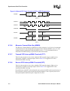
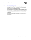
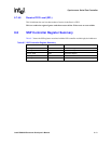
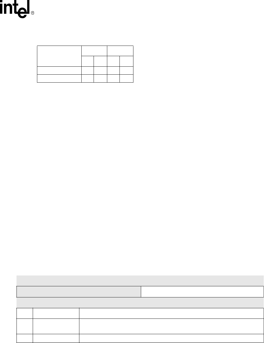
Table 8-4. TFT and RFT Values for DMA Servicing
DMA Burst Size TFT Value RFT Value
Min Max Min Max
8 Bytes 0 11 3 15
16 Bytes 0 7 7 15
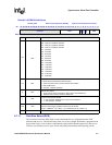
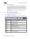
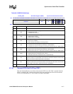
Table 8-5. SSDR Bit Definitions
0x4100_0010 SSP Data Register (SSDR) Synchronous Serial Port Controller
Bit
31 30 29 28 27 26 25 24 23 22 21 20 19 18 17 16 15 14 13 12 11 10 9 8 7 6 5 4 3 2 1 0
reserved Transmit/Receive Data
Reset
X 0x0000
Bits Name Description
15:0 Data
(Low Word)
Data word to be written to/read from Transmit/Receive FIFO
31:16 — reserved