


Intel® PXA255 Processor Developer’s Manual 9-1
I
2
C Bus Interface Unit 9
This chapter describes the Inter-Integrated Circuit (I2C) bus interface unit, including the operation
modes and setup for the PXA255 processor.
9.1 Overview
The I
2
C bus was created by the Phillips Corporation and is a serial bus with a two-pin interface.
The SDA data pin is used for input and output functions and the SCL clock pin is used to control
and reference the I
2
C bus. The I
2
C unit allows the processor to serve as a master and slave device
that resides on the I
2
C bus.
The I
2
C unit enables the processor to communicate with I
2
C peripherals and microcontrollers for
system management functions. The I
2
C bus requires a minimum amount of hardware to relay status
and reliability information concerning the processor subsystem to an external device.
The I
2
C unit is a peripheral device that resides on the processor internal bus. Data is transmitted to
and received from the I
2
C bus via a buffered interface. Control and status information is relayed
through a set of memory-mapped registers. Refer to The I
2
C-Bus Specification for complete details
on I
2
C bus operation.
Note: The I
2
C unit does not support the hardware general call, 10-bit addressing, or CBUS compatibility.
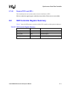
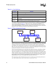
9.2 Signal Description
The I
2
C unit signals are SDA and SCL. Table 9-1 describes each signal’s function.
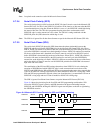
9.3 Functional Description
The I
2
C bus defines a serial protocol for passing information between agents on the I
2
C bus using a
two pin interface that consists of a Serial Data/Address (SDA) line and a Serial Clock Line (SCL).
Each device on the I
2
C bus is recognized by a unique 7-bit address and can operate as a transmitter
or as a receiver in master or slave mode. Table 9-2 lists the I
2
C operation modes.
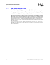
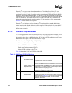
Table 9-1. I
2
C Signal Description
Signal Name Input/Output Description
SDA Bidirectional I
2
C Serial Data/Address signal
SCL Bidirectional I
2
C Serial Clock Line signal