


6-78 Intel® PXA255 Processor Developer’s Manual
Memory Controller
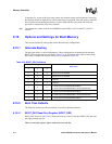
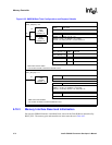
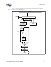
6.10.3 Memory Interface Reset and Initialization
On reset, the SDRAM Interface is disabled. Reset values for the Boot ROM are determined by
BOOT_SEL. The memory pins and controller are in the state shown in Table 6-42.
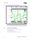
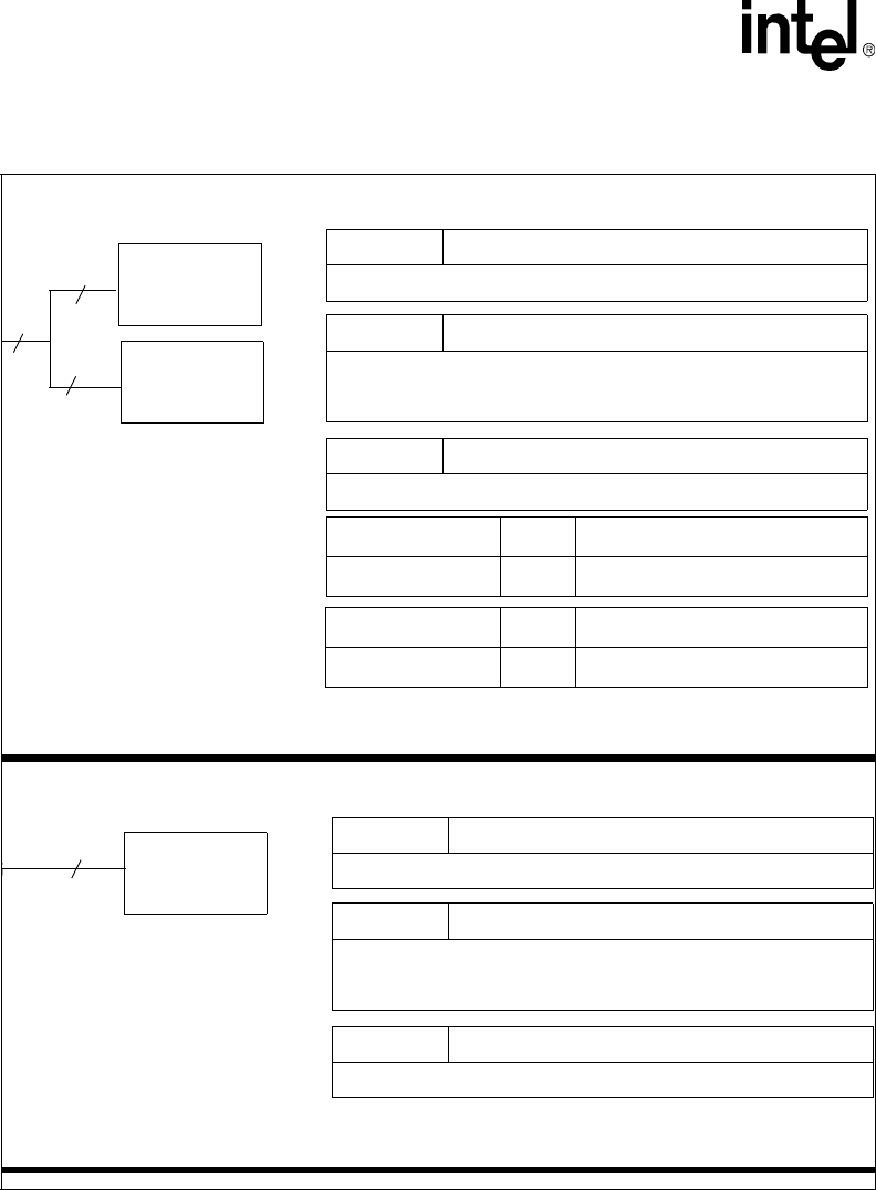
Figure 6-35. SMROM Boot Time Configurations and Register Defaults
BOOT_SEL[2:0] = 110
MSC0
SXCNFG
7FF0 7FF0
0004 4931
SXEN0 = 1h, SXCL0 = 4h (CL = 5),
SXRL0 = 1h (RL = 2), SXRA0 = 1h (13-bits),
SXCA0 = 2h (9-bits), SXTP0 = 0h, SXLATCH=1h
RBW0 = 0
MRS value must be 0061h.
BOOT_SEL[2:0] = 111
The number of banks in the device defaults to zero.
MDREFR 03CA 7FFF
E0PIN = 1, K0RUN = 1
SMROM
16-bit
(64 Mbit)
(nWORD = 0)
SMROM
16-bit
(64 Mbit)
(nWORD = 0)
16
16
32
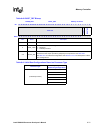
MSC0
SXCNFG
7FF0 7FF8
0004 4531
SXEN0 = 1h, SXCL0 = 4h (CL = 5),
SXRL0 = 1h (RL = 2), SXRA0 = 1h (13-bits),
SXCA0 = 1h (8-bits), SXTP0 = 0h, SXLATCH=1h
RBW0 = 1
MRS value must be 0061h.
The number of banks in the device defaults to zero.
MDREFR 03CA 7FFF
E0PIN = 1, K0RUN = 1
SMROM
16-bit
(32 Mbit)
(nWORD = 0)
16
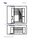
BOOT_SEL[2:0] = 100
BOOT_SEL[2:0] = 101
SXMRS
SXMRS
0232 0232
0232 0232
BOOT_SEL[2:0] = 110
BOOT_SEL[2:0] = 111
SXMRS
SXMRS
0232 0232
0232 0232