


6-48 Intel® PXA255 Processor Developer’s Manual
Memory Controller
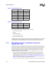
7:4 R/W RDFx<3:0>
ROM delay first access.
RDF programmed RDF value interpreted
0-11 0-11
12 13
13 15
14 18
15 23
Address to data valid for the first read access from all devices except VLIO
is equal to (RDFx + 2) memclks.
Address to data valid for subsequent read accesses to non-burst devices is
equal to (RDFx + 1) memclks.
nWE assertion for write accesses (which are non-burst) to all Flash is equal
to (RDFx + 1) memclks.
nOE (nPWE) assert time for each beat of read (write) is equal to (RDFx + 1)
memclks for Variable Latency I/O (nCS[5:0]). For Variable Latency I/O,
RDFx must be greater than or equal to 3.
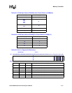
3R/WRBWx
ROM bus width
0 – 32 bits
1 – 16 bits
For reset value for RBW0, see Section 6.8.
This value must be programmed with all memory types including
Synchronous Static Memory.
This value must not change during normal operation.
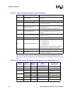
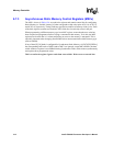
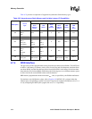
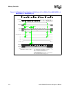
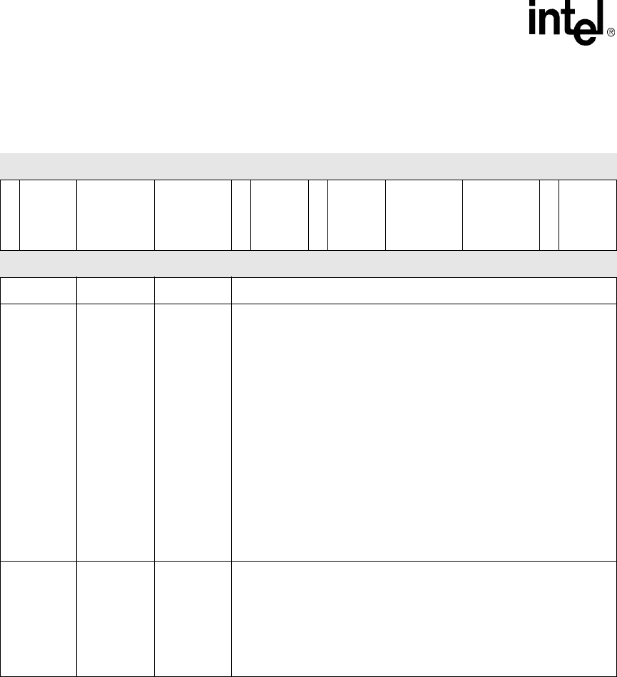
Table 6-24. MSC0/1/2 Bit Definitions (Sheet 2 of 3)
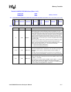
0x4800_0008
0x4800_000C
0x4800_0010
MSC0
MSC1
MSC2
Memory Controller
Bit
31 30 29 28 27 26 25 24 23 22 21 20 19 18 17 16 15 14 13 12 11 10 9 8 7 6 5 4 3 2 1 0
RBUFF1/3/5
RRR1/3/5 RDN1/3/5 RDF1/3/5
RBW1/3/5
RT1/3/5
RBUFF0/2/4
RRR0/2/4
RDN0/2/4 RDF0/2/4
RBW0/2/4
RT0/2/4
Reset
0 1 1 1 1 1 1 1 1 1 1 1 0 0 0 0 0 1 1 1 1 1 1 1 1 1 1 1 * 0 0 0
Bits Access Name Description