


Intel® PXA255 Processor Developer’s Manual 6-39
Memory Controller
6.6.4 Non-SDRAM Timing SXMEM Operation
Non-SDRAM Timing Synchronous Flash operation resets to asynchronous mode (page-mode for
reads and asynchronous single word writes). Software can change the Read Configuration Register
(RCR) to synchronous mode (burst-timing synchronous reads and asynchronous single word
writes). At boot time, the Non-SDRAM Timing Synchronous Flash operates similarly to an
asynchronous boot ROM (See Section 6.8).
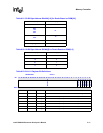
Consult the documentation for the memory being used. Table 6-17 is provided only as a reference.
The frequency configuration must be determined based on the CLK-to-output delay, the CLK
period, and the nADV-to-output delay timing parameters of the Flash device.
The values for this part number are shown as an example. For Intel part number 28F800F3,
programming values for this register to ensure proper operation with the processors are shown in
Table 6-17.
Software must ensure that the CLK-to-output delay is less than 1 SDCLK period for non-SDRAM
Timing Synchronous Flash.
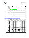
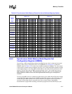
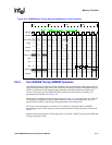
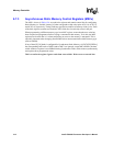
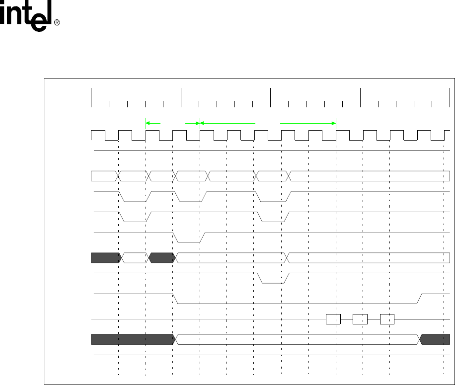
Figure 6-12. SMROM Read Timing Diagram Half-Memory Clock Frequency
NOP ACT NOP READ NOP STOP NOP
row col
d0 d1 d2
0000
CL = 5CL = 5RL = 2RL = 2
0ns 50ns 100ns 150ns
SDCLK
SDCKE
command
nCS[0]
nSDRAS
nSDCAS
MA[24:10]
nWE
nOE
MD
DQM[3:0]
RDnWR