


6-42 Intel® PXA255 Processor Developer’s Manual
Memory Controller
For divide-by-two mode, the following timing parameters apply:
• nADV assert time = 3 MEMCLKs
• MA, nCS setup to nADV asserted = 1 MEMCLK
• nADV deasserted to nOE asserted = (Code * 2) - 4 MEMCLKs
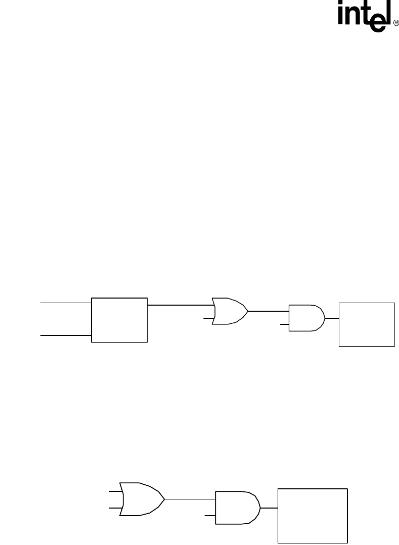
6.6.4.2 K3 Synchronous StrataFlash Reset
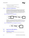
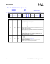
The PXA255 processor nRESET_OUT pin must be connected to the K3 #RST pin for Hardware
reset, Watchdog reset and sleep mode to work properly. GPIO reset however does not reset the
contents of the memory controller configuration register. If GPIO reset operation is required, a
state machine is necessary between nRESET, nRESET_OUT, GPIO[1], and #RST to ensure that
#RST is asserted during Hardware reset, Watchdog reset, and sleep mode, and not asserted during
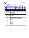
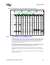
GPIO reset. Figure 6-14 shows the required logic. GPIO_a is an unused GPIO that is driven low by
software during the initialization sequence and left high during normal operation. After this is
completed, then enable GPIO reset.
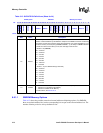
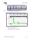
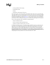
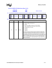
If Watchdog reset is not necessary, a secondary GPIO can control nRESET_OUT using the
equation #RST = nRESET & (nRESET_OUT | GPIO_a). This allows sleep mode entry to reset the
flash memory while keeping it in synchronous mode during a GPIO reset. Figure 6-15 shows the
required logic. GPIO_a is an unused GPIO that is kept high during normal operation and driven
low before sleep mode entry.
6.7 Asynchronous Static Memory
6.7.1 Static Memory Interface
The Static Memory interface is made up of six chip selects: nCS[5:0]. The chip selects can be
configured as the following:
Figure 6-14. Flash Memory Reset Using State Machine
nS
nR
GPIO[1]
GPIO_a
Q
nRESET_OUT
nRESET
#RST
K3 Flash
Figure 6-15. Flash Memory Reset Logic if Watchdog Reset is Not Necessary
GPIO_a
nRESET_OUT
nRESET
#RST
K3 Flash