


Intel® PXA255 Processor Developer’s Manual 3-5
Clocks and Power Manager
Note: These are the only supported frequency settings.
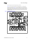
3.3.4 95.85 MHz Peripheral Phase Locked Loop
The 95.85 MHz PLL is the clock source for many of the peripheral blocks’ external interfaces.
These interfaces require ~48 MHz (UDC/USB, FICP), ~33 MHz (I
2
C), and ~20 MHz (MMC). The
generated frequency is not exactly the required frequency due to the chosen crystal and the lack of
a perfect Least Common Multiple between the units. The chosen frequencies keep each unit’s clock
frequency within the unit’s clock tolerance. If a crystal other than 3.6864 MHz is used, the clock
frequencies to the peripheral blocks’ interfaces may not yield the desired baud rates (or protocol’s
rate).
3.3.5 147.46 MHz Peripheral Phase Locked Loop
The 147.46 MHz PLL is the clock source for many of the peripheral blocks’ external interfaces.
These interfaces require ~14.75 MHz (UARTs), 12.288 MHz (AC97), and variable frequencies
(I
2
S). The generated frequency may not exactly match the required frequency due to the choice of
crystal and the lack of a perfect Least Common Multiple between the units. The chosen frequencies
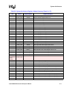
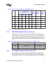
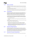
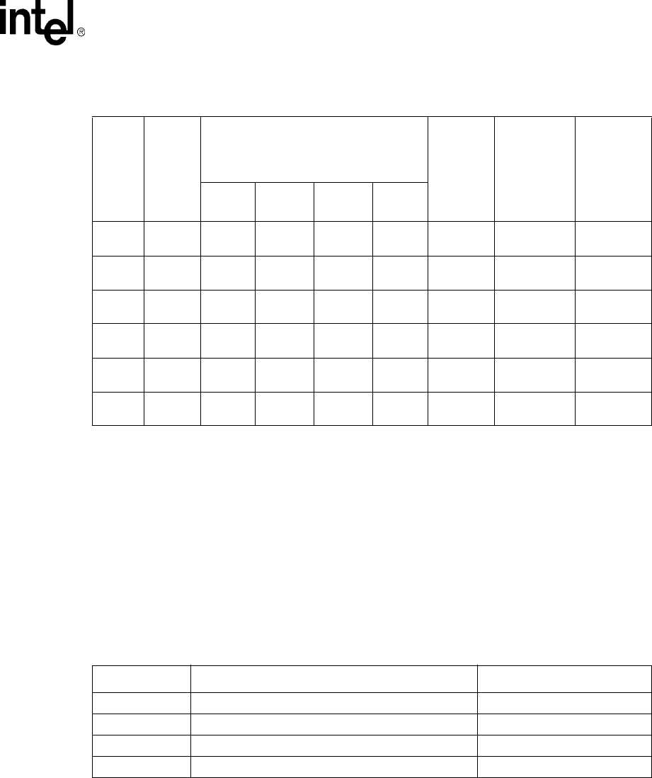
Table 3-1. Core PLL Output Frequencies for 3.6864 MHz Crystal
LM
Turbo Mode Frequency (MHz) for Values
“N” and Core Clock
Configuration Register (CCCR[15:0])
programming for Values of “N”
PXbus
Frequency
(MHz)
MEM, LCD
Frequency
(MHz)
SDRAM
max
Frequency
(MHz)
1.00
(Run)
1.50 2.00 3.00
27 1
99.5
@1.0 V
—
199.1
@1.0 V
298.6
@1.1 V
50 99.5 99.5
36 1
132.7
@1.0 V
— — — 66 132.7 66
27 2
199.1
@1.0 V
298.6
@1.1 V
398.1
@1.3 V
— 99.5 99.5 99.5
36 2
265.4
@1.1 V
— — — 132.7 132.7 66
45 2
331.8
@1.3 V
— — — 165.9 165.9 83
27 4
398.1
@1.3 V
— — — 196 99.5 99.5
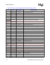
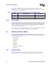
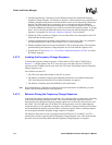
Table 3-2. 95.85 MHz Peripheral PLL Output Frequencies for 3.6864 MHz Crystal
Unit Name Nominal Frequency Actual Frequency
USB (UDC) 48 MHz 47.923 MHz
FICP 48 MHz 47.923 MHz
I
2
C 33 MHz 31.949 MHz
MMC 20 MHz 19.169 MHz