


16-2 Intel® PXA255 Processor Developer’s Manual
Network SSP Serial Port
16.3 Signal Description
Table 16-1 lists the external signals between the SSP serial ports and external device. If the port is
disabled, its pins are available for GPIO use. See Section 4.1, “General-Purpose I/O” for details on
configuring pin direction and Section 4.2, “Interrupt Controller” for Interrupt capabilities.
The Network SSP can output either NSSPTXD and NSSPRXD on either GPIO[83] or GPIO[84].
This allows a system to dynamically change the direction of transfer for this port. The NSSP can
change direction if enabled, but it must be idle.
16.4 Operation
The SSP controller transfers serial data between the PXA255 processor and an external device
through FIFOs. The PXA255 processor CPU initiates the transfers using programmed I/O or DMA
bursts to and from memory. Separate transmit and receive FIFOs and serial data paths permit
simultaneous transfers in both directions to and from the external device, depending on the
protocols chosen.
Programmed I/O transfers data directly between the CPU and the SSP Data Register (SSDR).
DMA transfers data between memory and the SSP Data Register (SSDR). Data written to the SSP
Data Register (by either the CPU or DMA) is automatically transmitted by the transmit FIFO. Data
received by the receive FIFO is automatically sent to the SSP Data Register.
16.4.1 Processor and DMA FIFO Access
The CPU or DMA accesses data through the SSP transmit and receive FIFOs. A CPU access takes
the form of programmed I/O, transferring one FIFO entry per access. The FIFO are seen as one 32-
bit location by the processor. CPU accesses are normally triggered by an SSSR interrupt and are
always 32-bits wide. CPU writes to the FIFOs ignore bits beyond the programmed FIFO data size
(EDSS/DSS value); and CPU reads return zeroes in the MSBs down to the programmed data size.
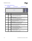
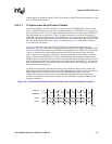
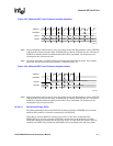
Table 16-1. SSP Serial Port I/O Signals
Name Direction Description
NSSPSCLK Input/Output
NSSPSCLK is the serial bit clock used to control the timing of a transfer.
NSSPSCLK is generated internally (master mode) or is supplied
externally (slave mode) as indicated by SSCR1[SCLKDIR] as defined in
Table 16-4.
NSSPSFRM Input/Output
NSSPSFRM is the serial frame indicator that indicates the beginning and
the end of a serialized data word. SSPSFRM is generated internally
(master mode) or is supplied externally (slave mode) as indicated by
SSCR1[SFRMDIR] as defined in Table 16-4.
NSSPTXD Output
NSSPTXD is the transmit data (serial data out) serialized data line. It is
available on two GPIO pins, GPIO[83] or GPIO[84]. See Section 4.1,
“General-Purpose I/O” for details.
NSSPRXD Input
NSSPRXD is the receive data (serial data in) serialized data line. It is
available on two GPIO pins, GPIO[83] or GPIO[84]. See Section 4.1,
“General-Purpose I/O” for details.