


Intel® PXA255 Processor Developer’s Manual 6-43
Memory Controller
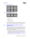
• Non-burst ROM or Flash memory
• Burst ROM or Flash
• SRAM
• SRAM-like variable latency I/O devices
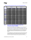
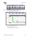
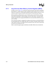
The Variable Latency I/O interface differs from SRAM in that it allows the use of the data-ready
input signal, RDY, to insert a variable number of memory-cycle wait states. The data bus width for
each chip-select region can be programmed as 16- or 32-bit. nCS[3:0] can also be configured for
Synchronous Static Memory (refer to Section 6.6). During Variable Latency I/O writes, nPWE is
used instead of nWE so SDRAM refreshes can be executed while performing the VLIO transfers.
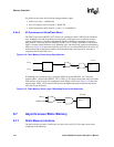
The use of the signals nOE, nWE, and nPWE is summarized below:
• nOE is asserted for all reads
• nWE is asserted for Flash and SRAM writes
• nPWE is asserted for Variable Latency I/O writes
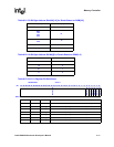
For SRAM and Variable Latency I/O implementations, DQM[3:0] signals are used for the write
byte enables, where DQM[3] corresponds to the MSB. The processor supplies 26-bits of byte
address for access of up to 64 Mbytes per chip select. This byte address is sent out on the 26
external address pins. Do not connect MA[1:0] for 32-bit systems. Do not connect MA[0] for 16-
bit systems (the PXA255 processor operating in 16-bit mode). For all reads on a 32 bit system
DQM[3:0] and MA[1:0] are 0. For all reads on a 16 bit system DQM[1:0] and MA[0] are 0. In the
timing diagrams, these byte addresses are shown and referred to as “addr”.