7-4 Intel® PXA255 Processor Developer’s Manual
LCD Controller
7.1.2 Pin Descriptions
When the LCD controller is enabled, all of the LCD pins are outputs only. When the LCD
controller is disabled, its pins can be use for general-purpose input/output (GPIO). Refer to the
System Integration Unit chapter for details.
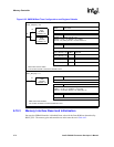
Table 7-1 describes the LCD controller’s pins. For more detailed information, see Section 7.3.5.
All of the LCD pins are outputs only.
7.2 LCD Controller Operation
7.2.1 Enabling the Controller
If the LCD controller is being enabled for the first time after system reset or sleep reset, all of the
LCD registers must be programmed as follows:
1. Configure the General Purpose I/O (GPIO) pins for LCD controller functionality. See
Chapter 4, “System Integration Unit” for details.
2. Write the frame descriptors and, if needed, the palette descriptor to memory.
3. Program all of the LCD configuration registers except the Frame Descriptor Address Registers
(FDADRx) and the LCD Controller Configuration Register 0 (LCCR0). See Section 7.6 for
details of all registers.
4. Program FDADRx with the memory address of the palette/frame descriptor, as described in
Section 7.6.5.2.
5. Enable the LCD controller by writing to LCCR0, as described in Section 7.6.1.
Table 7-1. Pin Descriptions
Pin Definition
L_DD[7:0]
These data lines transmit either four or eight data values at a time to the LCD display. For
monochrome displays, each pin value represents a single pixel. For passive color, groupings of
three pin values represent one pixel (red, green, and blue subpixel data values). In single-panel
monochrome mode, L_DD<3:0> pins are used. For double-pixel data, single-panel
monochrome, dual-panel monochrome, single-panel color, and active color modes, L_DD[7:0]
are used.
L_DD[15:8]
When dual-panel color or TFT (active color mode) operation is programmed, these data outputs
are also required to send pixel data to the screen.
L_PCLK
The Pixel Clock is used by the LCD display to clock the pixel data into the line shift register. In
passive mode, the pixel clock toggles only when valid data is available on the data pins. In
active mode, the pixel clock toggles continuously, and L_BIAS serves as an output to signal
when data is valid on the LCD’s data pins.
L_LCLK
The Line Clock is used by the LCD display to signal the end of a line of pixels. The display
transfers the line data from the shift register to the screen and increments the line pointer. In
active mode, it is the horizontal synchronization signal.
L_FCLK
The Frame Clock is used by the LCD display to signal the start of a new frame of pixels. The
display resets the line pointer to the top of the screen. In active mode, it is the vertical
synchronization signal.
L_BIAS
AC Bias is used to signal the LCD display to switch the polarity of the power supplies to the row
and column drivers of the screen to counteract DC offset. In active mode, it serves as the output
enable to signal when data is latched from the data pins using the Pixel Clock.


