


Intel® PXA255 Processor Developer’s Manual 6-59
Memory Controller
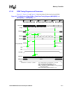
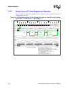
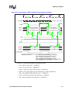
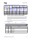
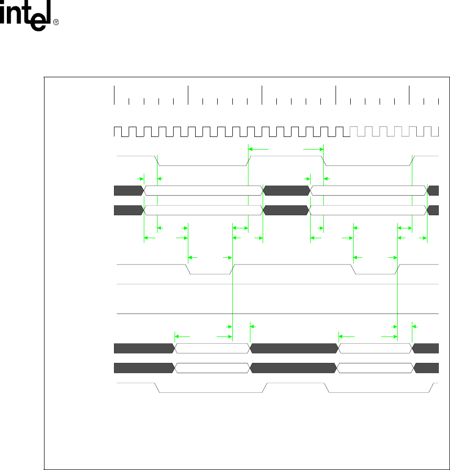
In Figure 6-23 some of the parameters are defined as follows:
• tAS = Address setup to nCS = 1 MEMCLK
• tCES = nCS setup to nWE = 2 MEMCLKs
• tASW = Address setup time to nWE asserted = 3 MEMCLKs
• tDSWH = Write data, DQM setup to nWE deasserted = (RDF+2) MEMCLKs
• tDH = Data, DQM hold after nWE deasserted = 1 MEMCLKs
• tCEH = nCS held asserted after nWE deasserted = 1 MEMCLK
• tAH = Address hold after nWE deasserted = 1 MEMCLKs
Figure 6-23. Asynchronous 32-Bit Flash Write Timing Diagram (2 Writes)
command address data address
'0' '0'
CMD DATA
"00" "00"
tDH
tDSWH
tDH
tDSWH
RDF+1
tAH
tCEH
RDF+1
tCES
tASW
RDF+1
tAH
tCEH
RDF+1
tCES
tASW
tAStAS
RRR*2+1RRR*2+1
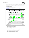
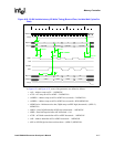
tAS = Address Setup to nCS asserted = 1 clk_mem
tAH = Address Hold from nWE deasserted = 2 clk_mem
tASW = Address Setup to nWE asserted = 3 clk_mem
tCES = nCS setup to nWE asserted = 2 clk_mems
tCEH = nCS hold from nWE deasserted = 1 clk_mem
tDSWH = MD/DQM setup to nWE deasserted = RDF+2 clk_mems
tDH = MD/DQM hold from nWE deasserted = 1 clk_mem
* A command and data write to Flash
MSC0:RDF0 = 2, RRR0 = 2
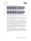
0ns 50ns 100ns 150ns 200ns
CLK_MEM
nCS[0]
MA[25:2]
MA[1:0]
nWE
nOE
RDnWR
MD[31:0]
DQM[3:0]
nADV(nSDCAS)