


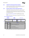
6-56 Intel® PXA255 Processor Developer’s Manual
Memory Controller
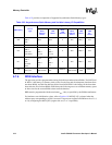
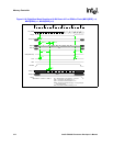
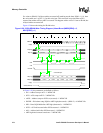
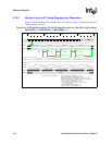
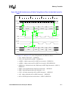
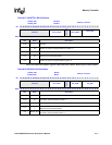
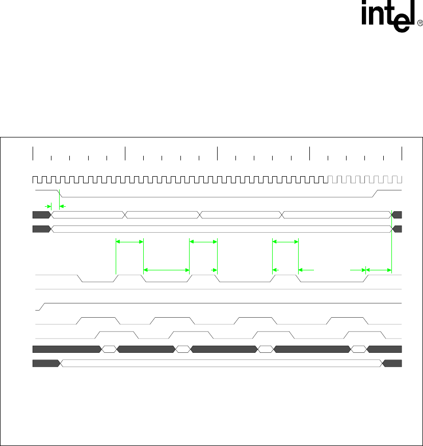
6.7.6.1 Variable Latency I/O Timing Diagrams and Parameters
Figure 6-21 shows the timing for Variable Latency I/O reads and Figure 6-22 shows the timing for
Variable Latency I/O writes.
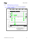
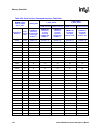
Figure 6-21. 32-Bit Variable Latency I/O Read Timing (Burst-of-Four, One Wait Cycle Per Beat)
(MSC0[RDF] = 2, MSC0[RDN] = 2, MSC0[RRR] = 1)
addr addr + 1 addr + 2 addr + 3
"00"
"0000"
RDF+1+Waits RRR*2+1
RDN+2
RDF+1+Waits
RDN+
RDF+1+Waits
RDN+2
RDF+1+Waits
RDN+
RDF+1+Waits
RDN
RDF+1+Waits
RDN+2
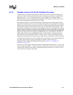
tAS
tAS = Address Setup to nCS asserted = 1 clk_mem
tAH = Address Hold from nOE deasserted = 1 clk_mem
tASRW0 = Address Setup to nOE asserted (1st access) = 3 clk_mems
tASRWn = Address Setup to nOE asserted (next access(s)) = RDN clk_mems
tCES = nCS setup to nOE asserted = 2 clk_mems
tCEH = nCS hold from nOE deasserted = 1 clk_mem
tDSOH = MD setup to Address changing = 1.5 clk_mems plus
board routing delays
tDOH = MD hold from Address changing = 0 ns
tRDYH = RDY Hold from nOE deasserted = 0 ns
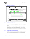
0 Waits
*MSC0: RDF0 = 3, RDN0 = 2, RRR0 = 1
1 Wait 2 Waits 3 Waits
0ns 100ns 200ns 300ns
CLK_MEM
nCS[0]
MA[25:2]
MA[1:0]
nOE
nPWE
RDnWR
RDY
RDY_sync
MD[31:0]
DQM[3:0]