7-20 Intel® PXA255 Processor Developer’s Manual
LCD Controller
The LCD pin timing changes when active mode is selected. Timing of each pin is described in
subsequent bit-field sections for both passive and active mode.
The LCD controller can be configured in active color display mode and used with an external DAC
and optionally an external palette to drive a video monitor. Only monitors that implement the RGB
data format can be used. The LCD controller does not support the NTSC standard. However, the
2X pixel clock mode allows the LCD controller to easily interface with an NTSC encoder, such as
the Analog Devices 7171 encoder.
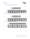
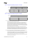
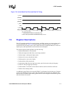
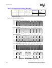
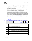
Figure 7-17 shows which bits are sent to the individual LCD data pins for both a frame buffer entry
(for 16-bit/pixel mode) and a selected palette entry (for 1, 2, 4 and 8 bit/pixel mode). The pixel bits
corresponding to L_DD pins when using an RGB format of 5:6:5 are also shown. In active mode,
L_DD pins [15:8] are also used. The user must configure the proper GPIO pins for LCD operation
to enable LCD Controller operation. See Chapter 4, “System Integration Unit” for GPIO
configuration information.
The processor LCD controller may be used with active panels having more than 16 data pins, but
the panel will be limited to a total of 64K colors. There are three options:
1. To maintain the panel’s full range of colors and increase the granularity of the spectrum,
connect the LCD controller’s 16 data pins to the panel’s most significant R, G, and B pixel data
input pins and tie the panel’s least significant R, G, and B data pins either high or low.
2. To maintain the granularity of the spectrum and limit the overall range of colors possible,
connect the LCD controller’s 16 data pins to the panel’s least significant R, G, and B pixel data
input pins and tie the panel’s most significant data pins either high or low.
3. Sometimes, better results can be obtained by replicating the upper bits on the lower bits.
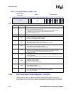
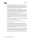
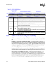
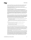
End of Frame Mask (EFM) — used to mask interrupt requests that are asserted at the end of each
frame (when the DMA length of transfer counter decrements to zero). When EFM=0, the interrupt
is enabled, and whenever the EOF status bit in the LCD status register (LCSR) is set to one, an
interrupt request is made to the interrupt controller. When EFM=1, the interrupt is masked, and the
state of the EOF status bit is ignored by the interrupt controller. Setting EFM does not affect the
current state of EOF or the LCD controller’s ability to set and clear EOF, it only blocks the
generation of the interrupt request.
Input Fifo Underrun Mask (IUM) — used to mask interrupt requests that are asserted whenever
an input FIFO underrun error occurs. When IUM=0, underrun interrupts are enabled, and whenever
an input FIFO underrun (IUL, IUU) status bit in the LCD status register (LCSR) is set to one, an
interrupt request is made to the interrupt controller. When IUM=1, underrun interrupts are masked
and the state of the underrun status bits (IUL, IUU) is ignored by the interrupt controller. Setting
IUM does not affect the current state of these status bits or the LCD controller’s ability to set and
clear them, it only blocks the generation of the interrupt requests.
Start Of Frame Mask (SFM) — used to mask interrupt requests that are asserted at the beginning
of each frame when the LCD’s frame descriptor has been loaded into the internal DMA registers.
When SFM=0, the interrupt is enabled, and whenever the start of frame (SOF) status bit in the LCD
Figure 7-17. Frame Buffer/Palette Output to LCD Data Pins in Active Mode
4/8/16 Bits/Pixel Mode, Frame Buffer or Palette Entry
PIxelR4R3R2R1R0G5G4G3G2G1G0B4B3B2B1B0
Bit1514131211109876543210
L_DD
Pin
1514131211109876543210


