


Intel® PXA255 Processor Developer’s Manual 11-11
Fast Infrared Communication Port
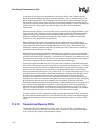
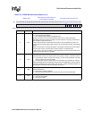
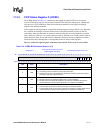
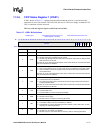
11.3.3 FICP Control Register 2 (ICCR2)
The ICCR2, shown in Table 11-4, contains two bit fields that control the polarity of the transmit
and receive data pins and two bits that determine the trigger level for the receive FIFO. The FICP
must be disabled (RXE=TXE=0) when these bits are changed.
This is a read/write register. Ignore reads from reserved bits. Write zeros to reserved bits.
Table 11-4. ICCR2 Bit Definitions
0x4080_0008
Fast Infrared Communication Port
Control Register 2 (ICCR2)
Fast Infrared Communication Port
Bit
31 30 29 28 27 26 25 24 23 22 21 20 19 18 17 16 15 14 13 12 11 10 9 8 7 6 5 4 3 2 1 0
reserved
RXP
TXP
TRIG
Reset 0 0 0 0 0 0 0 0 0 0 0 0 0 0 0 0 0 0 0 0 0 0 0 0 0 0 0 0 1 1 0 0
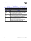
Bits Name Description
[31:4] — reserved
3RXP
Receive pin polarity select.
0 = Data from the receive data pin is inverted before being used by the FICP unit.
1 = Data from the receive data pin to the FICP unit is not inverted.
Set on reset.
2TXP
Transmit pin polarity select.
0 = Data from the FICP is inverted before being sent to the transmit data pin.
1 = Data from the FICP is not inverted before being sent to the transmit data pin.
Set on reset.
[1:0] TRIG
Receive FIFO trigger level
The receive FIFO generates service requests when the FIFO has reached the trigger level
and has no errors in its data. The DMA controller data transfer size must be set to the same
size as the Receive FIFO trigger level. To change the trigger level, the Receive FIFO must
be disabled.
0b00- receive FIFO service request is generated when the FIFO has 8 bytes or more
0b01- receive FIFO service request is generated when the FIFO has 16 bytes or more
0b10- receive FIFO service request is generated when the FIFO has 32 bytes or more
0b11- reserved