


10-6 Intel® PXA255 Processor Developer’s Manual
UARTs
.
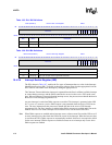
10.4.2.1 Receive Buffer Register (RBR)
In non-FIFO mode, the RBR, shown in Table 10-3, holds the character received by the UART’s
Receive Shift Register. If the RBR is configured to use fewer than eight bits, the bits are right-
justified and the most significant bits (MSB) are zeroed. Reading the register empties the register
and clears the Data Ready (DR) bit in the Line Status Register (LSR) to a 0.
In FIFO mode, the RBR latches the value of the data byte at the front of the FIFO.
This is a read-only register. Ignore reads from reserved bits.
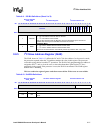
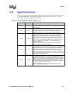
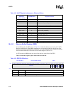
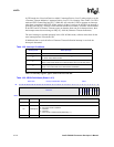
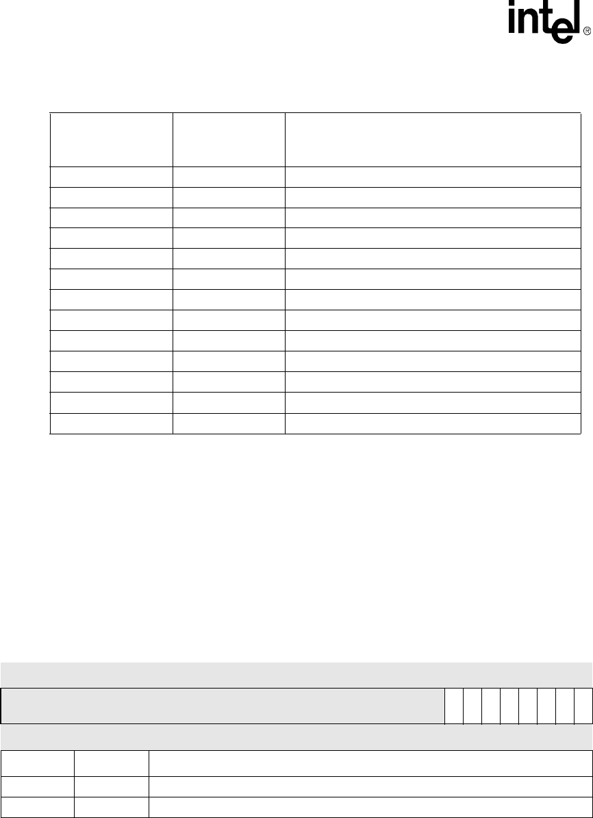
Table 10-2. UART Register Addresses as Offsets of a Base
UART Register
Addresses
(Base + offset)
DLAB Bit Value Register Accessed
Base 0 Receive Buffer (read only)
Base 0 Transmit Buffer (write only)
Base + 0x04 0 Interrupt Enable (read/write)
Base + 0x08 X Interrupt Identification (read only)
Base + 0x08 X FIFO Control (write only)
Base + 0x0C X Line Control (read/write)
Base + 0x10 X Modem Control (read/write)
Base + 0x14 X Line Status (read only)
Base + 0x18 X Modem Status (read only)
Base + 0x1C X Scratch Pad (read/write)
Base + 0x20 X Infrared Selection (read/write)
Base 1 Divisor Latch Low (read/write)
Base + 0x04 1 Divisor Latch High (read/write)
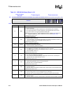
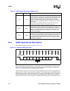
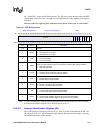
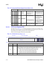
Table 10-3. RBR Bit Definitions
Base (DLAB=0) Receive Buffer Register UART
Bit
31 30 29 28 27 26 25 24 23 22 21 20 19 18 17 16 15 14 13 12 11 10 9 8 7 6 5 4 3 2 1 0
reserved
RBR7
RBR6
RBR5
RBR4
RBR3
RBR2
RBR1
RBR0
Reset 0 0 0 0 0 0 0 0 0 0 0 0 0 0 0 0 0 0 0 0 0 0 0 0 0 0 0 0 0 0 0 0
Bits Name Description
31:8 — reserved
7:0 RBR[7:0] Data byte received least significant bit first.