


7-32 Intel® PXA255 Processor Developer’s Manual
LCD Controller
7.6.5 LCD Controller DMA
The LCD controller has two fully independent DMA channels used to transfer both the palette
buffer and the frame buffer from external memory to the LCD controller. The LCD DMA
controller (DMAC) behaves much like the processor DMAC in descriptor fetch mode. DMA
channel 0 is used for single-panel display mode and the upper screen in dual-panel mode. DMA
channel 1 is used exclusively for the lower screen in dual-panel mode. The palette RAM is always
loaded through DMA channel 0. All of the information for the DMA transfers is maintained in
registers within the LCD DMAC. These registers are loaded from frame descriptors located in
main memory. One descriptor must be used per frame buffer in memory. A separate descriptor is
also used when the palette RAM is loaded. Multiple descriptors can be chained together in a list,
making it possible for the DMAC to transfer data from an essentially infinite number of
discontiguous locations. The four DMA register types are numbered according to the associated
DMA channel: See Section 7.6.5.2, Section 7.6.5.3, Section 7.6.5.4, and Section 7.6.5.5 for more
information.
7.6.5.1 Frame Descriptors
Although the FDADRx registers are loaded by software, the other DMA registers can only be
loaded indirectly from DMA frame descriptors. A frame descriptor is a four-word block, aligned on
a 16-byte boundary, in main memory:
word[0] contains the value for FDADRx
19:16 API
AC bias Pin transitions per Interrupt.
Value (0–15) is used to specify the number of AC bias pin transitions to count before setting
the line count status (ABC) bit, signalling an interrupt request. The counter is frozen when
ABC is set and is restarted when ABC is cleared by software. This function is disabled
when API=0x0.
15:8 ACB
AC Bias pin frequency:
In passive-display mode (LCCR0[PAS]=0), value (0–255) specifies the number of line
clocks to count before toggling the AC bias pin. This pin is used to periodically invert the
polarity of the power supply to prevent D.C. charge buildup within the display. If the passive
display being controlled does not need to use L_BIAS, program ACB to its maximum value
(0xFF) to conserve power. ACB can be used in conjunction with API to count line clocks in
active mode (LCCR0[PAS] = 1).
Number of line clocks/toggle of the L_BIAS pin = (ACB+1)
7:0 PCD
Pixel Clock Divisor:
Value (0–255) is used to specify the frequency of the pixel clock based on the LCD/Memory
Controller clock (LCLK) frequency. The Pixel clock frequency can range from LCLK/2 to
LCLK/512.
Pixel Clock Frequency = LCLK/(2*(PCD+1)).
PCD must be programmed with a value of 1 or greater if Double Pixel Clock Mode is
enabled.
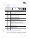
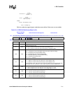
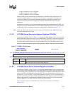
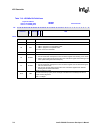
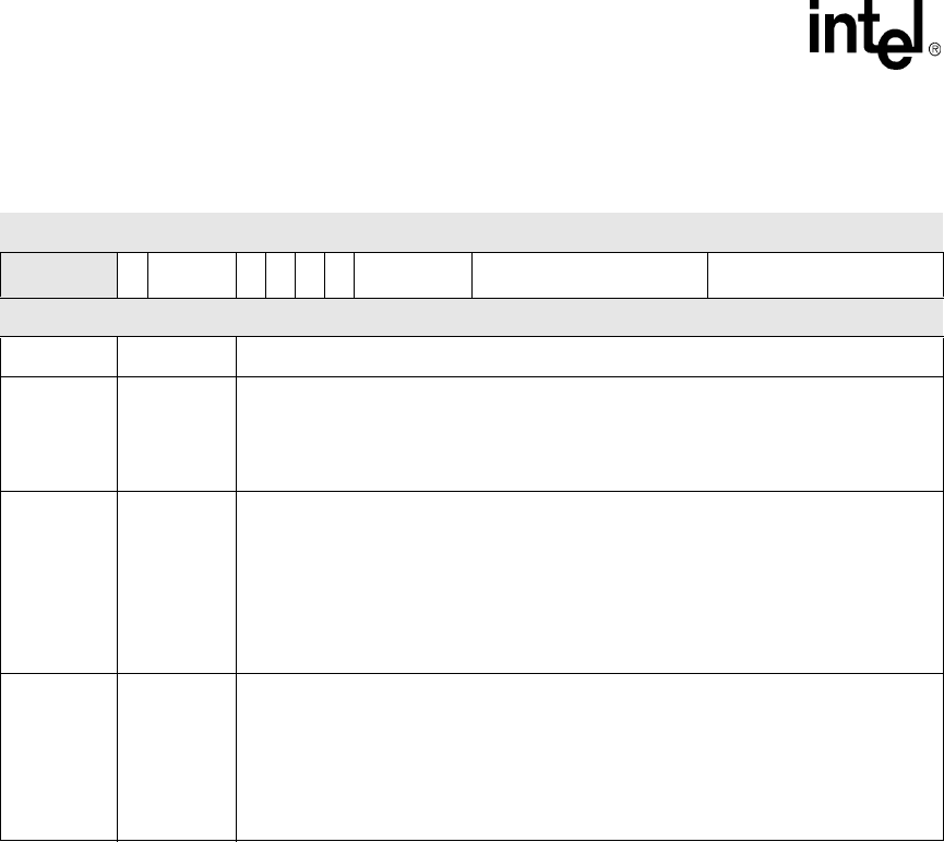
Table 7-6. LCCR3 Bit Definitions (Sheet 2 of 2)
Physical Address
0x4400_000C
LCD Controller Control Register 3 LCD Controller
Bit
31 30 29 28 27 26 25 24 23 22 21 20 19 18 17 16 15 14 13 12 11 10 9 8 7 6 5 4 3 2 1 0
reserved
DPC
BPP
OEP
PCP
HSP
VSP
API ACB PCD
Reset
X X X X 0 0 0 0 0 0 0 0 0 0 0 0 0 0 0 0 0 0 0 0 0 0 0 0 0 0 0 0
Bits Name Description