


6-74 Intel® PXA255 Processor Developer’s Manual
Memory Controller
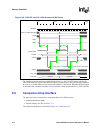
is deasserted or, as part of the sleep entry routine, the alternate master can be disabled. If necessary,
the alternate master can hold the bus until its transaction is completed. After the memory controller
has completed all outstanding transactions, it places SDRAM into self-refresh and allows the
processor to complete the sleep entry sequence.
Note: The alternate bus master must de-assert MBREQ when nVDD_FAULT or nBATT_FAULT is
asserted.
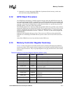
6.10 Options and Settings for Boot Memory
This section explains the settings that control Boot Memory configurations.
6.10.1 Alternate Booting
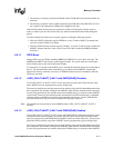
The processor allows six boot configurations. These configurations are determined by the three
BOOT_SEL(2:0) pins and are described in Table 6-39. A description of the effect of these input
pins on the Configuration registers at boot time is included in Section 6.8.
6.10.2 Boot Time Defaults
The following sections provide information on boot time default parameters.
6.10.2.1 BOOT_DEF Read-Only Register (BOOT_DEF)
BOOT_DEF, shown in Table 6-40, contains the boot-up values for the three BOOT_SEL pins and
the single package-type bit.
This is a read-only register. Ignore reads from reserved bits.
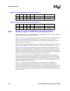
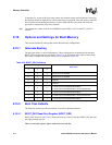
Table 6-39. BOOT_SEL Definitions
BOOT_SEL
Boot From...
210
0 0 0 Asynchronous 32-bit ROM
0 0 1 Asynchronous 16-bit ROM
0 1 0 reserved
0 1 1 reserved
100
1- 32-bit Synchronous Mask ROM (64 Mbit)
2- 16-bit Synchronous Mask ROMs = 32 bits (32 Mbit each)
1 0 1 1- 16-bit Synchronous Mask ROM (64 Mbit)
1 1 0 2- 16-bit Synchronous Mask ROMs = 32 bits (64 Mbit each)
1 1 1 1- 16-bit Synchronous Mask ROM (32 Mbit)