


16-8 Intel® PXA255 Processor Developer’s Manual
Network SSP Serial Port
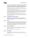
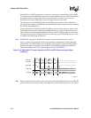
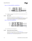
When SPH is set, SSPSCLK remains in its inactive or idle state (as determined by SSCR1[SPO])
for one-half cycle after SSPSFRM is asserted low at the beginning of a frame. SSPSCLK continues
to transition for the remainder of the frame and is then held in its inactive state for one full
SSPSCLK period before SSPSFRM is de-asserted high at the end of the frame.
The combination of the SSCR1[SPO] and SSCR1[SPH] settings determine when SSPSCLK is
active during the assertion of SSPSFRM and which SSPSCLK edge transmits and receives data on
the SSPTXD and SSPRXD pins.
When programming SSCR1[SPO] and SSCR1[SPH] to the same value (both set or both cleared),
transmit data is driven on the falling edge of SSPSCLK and receive data is latched on the rising
edge of SSPSCLK. When programming SSCR1[SPO] and SSCR1[SPH] to opposite values (one
set and the other cleared), transmit data is driven on the rising edge of SSPSCLK and receive data
is latched on the falling edge of SSPSCLK.
Note: SSCR1[SPH] is ignored for all data frame formats except for the Motorola SPI* protocol.
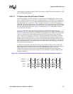
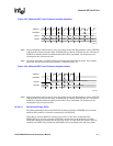
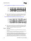
Figure 16-6 shows the pin timing for all four programming combinations of SSCR1[SPO] and
SSCR1[SPH]. The SSCR1[SPO] inverts the polarity of the SSPSCLK signal and SSCR1[SPH]
determines the phase relationship between SSPSCLK and SSPSFRM, shifting the SSPSCLK
signal one-half phase to the left or right during the assertion of SSPSFRM.
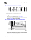
Note: When configured as either master or slave (to clock or frame) the SSP continues to drive SSPTXD
with the last bit of data sent (the LSB). If SSCR0[SSE] is cleared, SSPTXD goes low. The state of
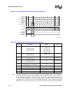
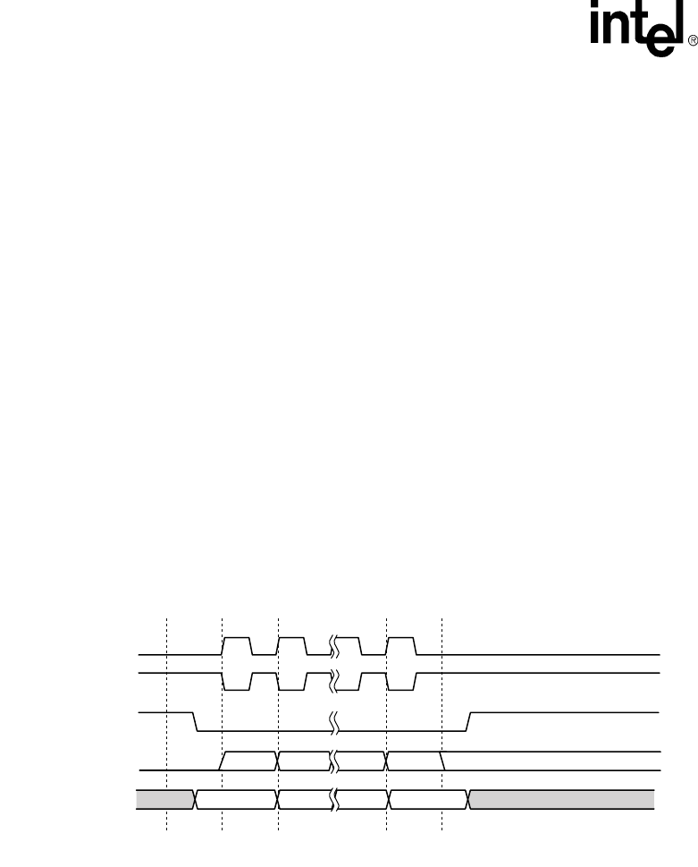
Figure 16-5. Motorola SPI* Frame Protocols for SPO and SPH Programming (multiple
transfers)
A9652-01
SSPRXD
SSPSFRM
SSPSCLK
SPO=0
SSPSCLK
SPO=1
SSPTXD
MSB 4 to 32 Bits LSB
Bit[N] Bit[N-1] Bit[1] Bit[0]
Bit[N] Bit[N-1] Bit[1] Bit[0]
Undefined
Undefined
End of Transfer Data State