8-10 Intel® PXA255 Processor Developer’s Manual
Synchronous Serial Port Controller
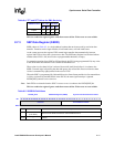
transmit FIFO. The transmit logic in the SSPC left-justifies the data sample according to the DSS
bits before the sample is transmitted. Data sizes of 1, 2, and 3 bits are reserved and produce
unpredictable results in the SSPC.
In National Microwire frame format, this bit field selects the size of the received data. The size of
the transmitted command data is either 8-bit or 16-bit as selected by the MWDS bit in SSCR1.
8.7.1.2 Frame Format (FRF)
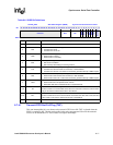
The 2-bit frame format (FRF) field is used to select Motorola SPI (FRF=00), Texas Instruments
Synchronous Serial (FRF=01), or National Microwire (FRF=10) frame format.
FRF=11 is reserved and the SSPC produces unpredictable results if this value is used.
8.7.1.3 External Clock Select (ECS)
The external clock select (ECS) bit determines whether the SSPC uses the on-chip 3.6864-MHz
clock or an off-chip clock supplied via SSPEXTCLK. When ECS=0, the SSPC uses the on-chip
3.6864-MHz clock to produce a range of serial transmission rates from 7.2 Kbps to 1.8432 Mbps.
When ECS=1, the SSP uses SSPEXTCLK to access an off-chip clock. The off-chip clock’s
frequency can be any value up to 3.6864 MHz. The off-chip clock is useful when a serial
transmission rate not evenly divisible from 3.6864 MHz is required for synchronization with the
target off-chip slave device.
If the off-chip clock is used, the user must set the appropriate bits in the GPIO alternate function
and pin direction registers that correspond to the pin. See Chapter 4, “System Integration Unit” for
more details on configuring GPIO pins for alternate functions.
Note: Disable the SSPC by setting the SSPC Enable (SSE) to a 0 before setting the ECS bit to a 1. The
ECS bit may be set to one either before the SSE is set to one or at the same time.
8.7.1.4 Synchronous Serial Port Enable (SSE)
The SSCR0[SSE] bit is used to enable and disable all SSP operations. When SSCR0[SSE]=0, the
SSP is disabled. When SSCR0[SSE]=1, the SSP is enabled. When the SSP is disabled, all of its
clocks are powered down to minimize power consumption.The SSP is disabled following a reset.
When the SSCR0[SSE] bit is cleared during active operation, the SSP is immediately disabled and
the frame being transmitted is terminated. Clearing SSCR0[SSE] resets the SSP’s FIFOs and the
SSP status bits. The SSP’s control registers are not reset when SSCR0[SSE] is cleared.
Note: After reset or after the SSCR0[SSE] is cleared, ensure that the SSCR1 and SSSR registers are
properly reconfigured or reset before re-enabling the SSP with the SSCR0[SSE]. Other control bits
in SSCR0 may be written at the same time as the SSCR0[SSE].
When the SSPC is disabled, its five pins may be used as GPIOs. They are configured as inputs or
outputs with the control registers described in Chapter 4, “System Integration Unit”. In Sleep
mode, the pins’ states are controlled by the GPIO sleep register. SSPC register settings have no
effect on the pins in Sleep mode.


