


4-8 Intel® PXA255 Processor Developer’s Manual
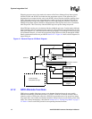
System Integration Unit
This is read/write register. Ignore reads from reserved bits. Write zeros to reserved bits.
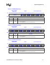
4.1.3.2 GPIO Pin Direction Registers (GPDR0, GPDR1, GPDR2)
GPDR0, GPDR1, GPDR2, shown in Table 4-6, Table 4-7, and Table 4-8, control whether a pin is
an input or an output. The GPDR contain one direction control bit for each of the 85 GPIO pins. If
a direction bit is programmed to a one, the GPIO is an output. If it is programmed to a zero, it is an
input. Reserved bits must be written to zeros and reads to the reserved bits must be ignored.
Note: A reset clears all bits in the GPDR0-2 registers and configures all GPIO pins as inputs.
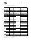
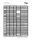
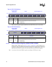
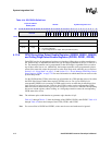
Table 4-4. GPLR1 Bit Definitions
Physical Address
0x40E0_0004
GPLR1 System Integration Unit
Bit
31 30 29 28 27 26 25 24 23 22 21 20 19 18 17 16 15 14 13 12 11 10 9 8 7 6 5 4 3 2 1 0
PL63
PL62
PL61
PL60
PL59
PL58
PL57
PL56
PL55
PL54
PL53
PL52
PL51
PL50
PL49
PL48
PL47
PL46
PL45
PL44
PL43
PL42
PL41
PL40
PL39
PL38
PL37
PL36
PL35
PL34
PL33
PL32
Reset 0 0 0 0 0 0 0 0 0 0 0 0 0 0 0 0 0 0 0 0 0 0 0 0 0 0 0 0 0 0 0 0
Bits Name Description
<31:0> PL[x]
GPIO Pin Level ‘x’ (where x = 32 to 63).
This read-only field indicates the current value of each GPIO.
0 – Pin state is low
1 – Pin state is high
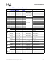
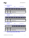
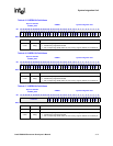
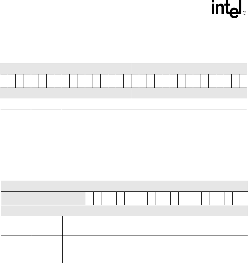
Table 4-5. GPLR2 Bit Definitions
Physical Address
0x40E0_0008
GPLR2 System Integration Unit
Bit
31 30 29 28 27 26 25 24 23 22 21 20 19 18 17 16 15 14 13 12 11 10 9 8 7 6 5 4 3 2 1 0
reserved
PL84
PL83
PL82
PL81
PL80
PL79
PL78
PL77
PL76
PL75
PL74
PL73
PL72
PL71
PL70
PL69
PL68
PL67
PL66
PL65
PL64
Reset 0 0 0 0 0 0 0 0 0 0 0 0 0 0 0 0 0 0 0 0 0 0 0 0 0 0 0 0 0 0 0 0
Bits Name Description
<31:21> — reserved
<20:0> PL[x]
GPIO Pin Level ‘x’ (where x = 64 to 84).
This read-only field indicates the current value of each GPIO.
0 – Pin state is low
1 – Pin state is high