


4-36 Intel® PXA255 Processor Developer’s Manual
System Integration Unit
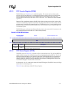
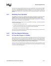
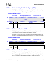
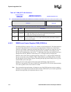
4.4.2.2 OS Timer Interrupt Enable Register (OIER)
The OIER, shown in Table 4-42, contains four enable bits that indicate whether a match between
one of the match registers and the OS timer counter sets a status bit in the OSSR. Each match
register has a corresponding enable bit. Clearing an enable bit does not clear the corresponding
interrupt status bit if it is already set.
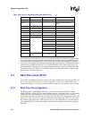
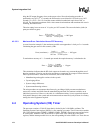
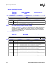
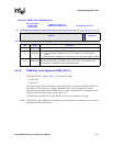
Table 4-41. OSMR[x] Bit Definitions
Physical Address
0x40A0_0000
0x40A0_0004
0x40A0_0008
0x40A0_000C
OS Timer Match Register 0-3
(OSMR3, OSMR2, OSMR1,
OSMR0)
System Integration Unit
Bit
31 30 29 28 27 26 25 24 23 22 21 20 19 18 17 16 15 14 13 12 11 10 9 8 7 6 5 4 3 2 1 0
OSMV
Reset
0 0 0 0 0 0 0 0 0 0 0 0 0 0 0 0 0 0 0 0 0 0 0 0 0 0 0 0 0 0 0 0
Bits Name Description
<31:0> OSMV
OS Timer Match Value.
The value compared against the OS timer counter.
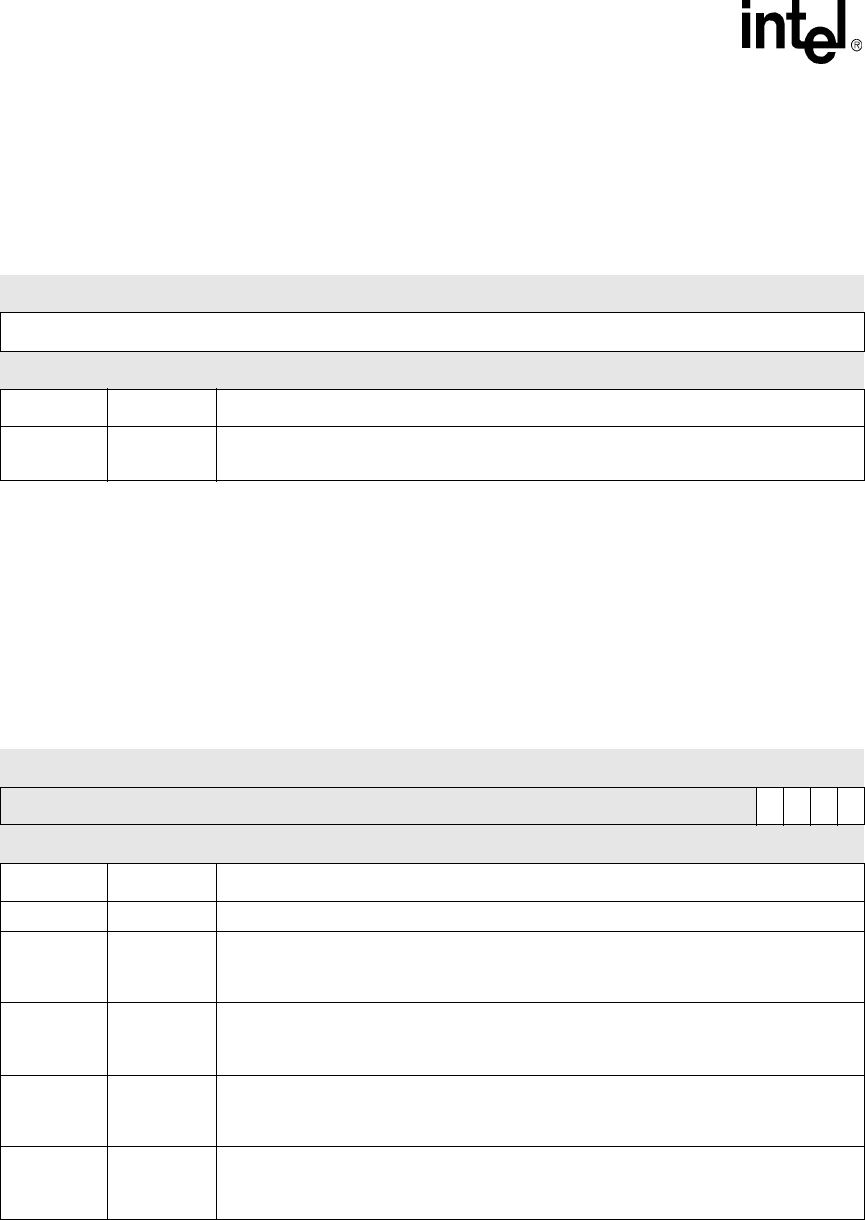
Table 4-42. OIER Bit Definitions
Physical Address
0x40A0_001C
OS Timer Interrupt Enable
Register (OIER)
System Integration Unit
Bit
31 30 29 28 27 26 25 24 23 22 21 20 19 18 17 16 15 14 13 12 11 10 9 8 7 6 5 4 3 2 1 0
reserved
E3
E2
E1
E0
Reset ? ? ? ? ? ? ? ? ? ? ? ? ? ? ? ? ? ? ? ? ? ? ? ? ? ? ? ? 0 0 0 0
Bits Name Description
<31:4> — reserved
<3> E3
Interrupt enable channel 3.
0 – A match between OSMR3 and the OS Timer will NOT assert OSSR[M3].
1 – A match between OSMR3 and the OS Timer asserts OSSR[M3].
<2> E2
Interrupt enable channel 2.
0 – A match between OSMR2 and the OS Timer will NOT assert OSSR[M2].
1 – A match between OSMR2 and the OS Timer asserts OSSR[M2].
<1> E1
Interrupt enable channel 1.
0 – A match between OSMR1 and the OS Timer will NOT assert OSSR[M1].
1 – A match between OSMR1 and the OS Timer asserts OSSR[M1].
<0> E0
Interrupt enable channel 0.
0 – A match between OSMR0 and the OS Timer will NOT assert OSSR[M0].
1 – A match between OSMR0 and the OS Timer asserts OSSR[M0].