


6-54 Intel® PXA255 Processor Developer’s Manual
Memory Controller
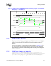
For writes to SRAM, if all byte enables are turned off (masking out the data, DQM = 1111), then
the write enable are 1 (nWE = 1) for this write beat. This can result in a period when nCS is
asserted, but neither nOE nor nWE is asserted. This happens with a write of 1 beat to SRAM, but
all byte enables are turned off.
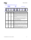
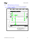
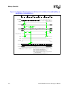
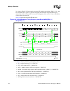
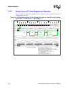
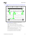
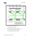
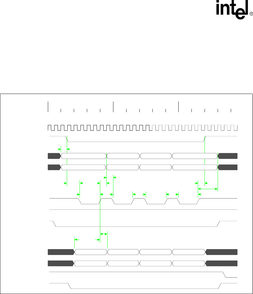
Figure 6-20 shows the timing for SRAM writes.
In Figure 6-20, the parameters are defined as follows:
• tAS = Address setup to nCS = 1 MEMCLK
• tCES = nCS setup to nWE = 2 MEMCLKs
• tASW = Address setup to nWE low (asserted) = 1 MEMCLK
• tDSWH = Write data setup, DQM to nWE high (deasserted) = (RDN+2) = 4 MEMCLKs
• tDH = Data, DQM hold after nWE high (deasserted) = 1 MEMCLK
• tCEH = nCS held asserted after nWE deasserted = 1 MEMCLK
• tAH = Address hold after nWE deasserted = 1 MEMCLK
• nWE high time between burst beats = 2 MEMCLKs
Figure 6-20. 32-Bit SRAM Write Timing Diagram (4-beat Burst (MSC0[RDN] = 2,
MSC0[RRR] = 1)
0 1 2 3
byte addr byte addr byte addr byte addr
D0 D1 D2 D3
mask0 mask1 mask2 mask3
tDH
tDSWH
tCEH
RDN+1
RRR*2+1
RDN+1RDN+1RDN+1RDN+1
tASW
RDN+1
tAH
RDN+1
tCES
RDN
tAS
mask data bytes
MEMCLK
nCS[0]
MA[25:2]
MA[1:0]
nWE
nOE
RDnWR
MD[31:0]
DQM[3:0]
nCS[1]
nADV(nSDCAS)